FMC Mezzanine Ecosystem: Extend Analog and High-Speed I/O with VITA 57
FPGA dev boards never have enough I/O: you need a high-speed ADC, an optical module, or LVDS sensors — and you don’t want to redesign the PCB every time. FMC (FPGA Mezzanine Card, VITA 57 standard) solves this: one carrier board + a library of standard mezzanine cards, swap the card to change the interface. This article walks through LPC vs HPC, pin budget, and common mezzanine configurations.
1. What Is FMC: A Standard Interface Between Carrier and Mezzanine
FMC was published by the VITA consortium in 2008 (VITA 57). The core idea:
- Carrier: FPGA + DDR + PCIe core resources, fixed long-term
- Mezzanine: ADC/DAC, fiber, HDMI, LVDS I/O modules, swap as needed
- Connector: high-speed board-to-board connector carrying signals, clocks, and power
One carrier with different mezzanines becomes a data acquisition card, SDR platform, or video processing board — no PCB redesign, no revalidation.
2. LPC vs HPC: Choosing the Pin Budget
FMC comes in two sizes, differing in transceivers and total I/O count:
| Item | FMC LPC (Low Pin Count) | FMC HPC (High Pin Count) |
|---|---|---|
| High-speed transceivers (GTP/GTX/GTH) | 2 pairs | 10 pairs (8~10 usable) |
| Single-ended I/O pins | ≤ 34 pairs | ≤ 80 pairs |
| Differential I/O pins | ≤ 17 pairs | ≤ 40 pairs |
| Total I/O | ≈ 68 | ≈ 160 |
| Clock pairs | 1 pair | 2 pairs |
| Use cases | Low-speed ADC, LVDS sensors, basic expansion | High-speed ADC/DAC, fiber, multi-channel high-speed I/O |
Rule: count transceivers first
If your mezzanine needs more than 2 transceiver pairs (e.g., 4-channel 1Gsps ADC, QSFP fiber module), go HPC. LPC only has 2 transceivers — a high-speed mezzanine won’t run to spec.
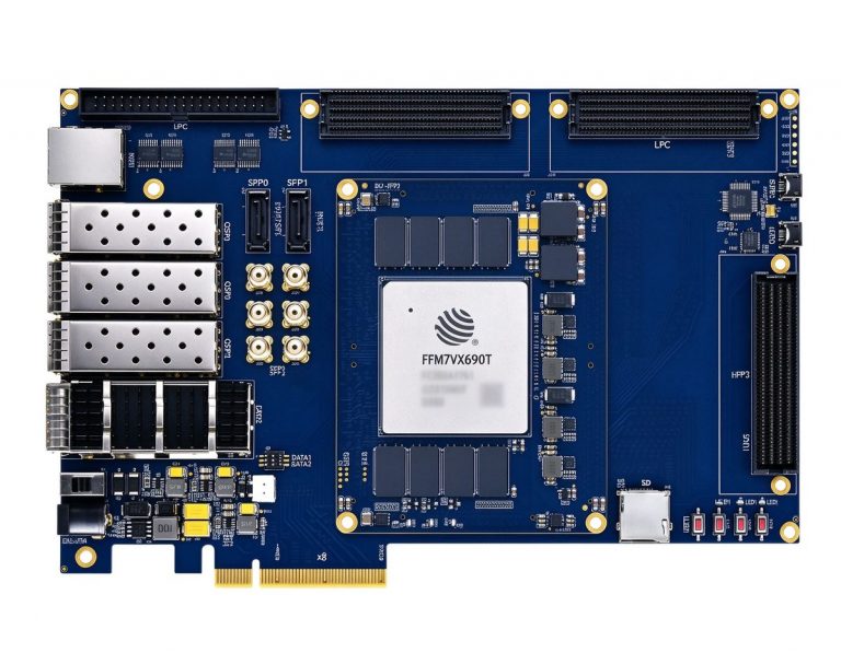
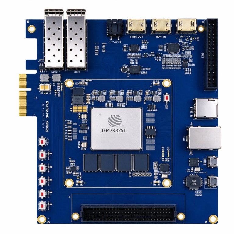
Duyuan carrier boards:
- DUF7690T: dual FMC HPC (2×10 transceiver pairs) — multi-channel high-speed mezzanines
- DUK7325T: single FMC HPC — cost-effective choice
- PBC7K325G: single FMC LPC — entry-level expansion
3. How FMC Pins Are Organized
FMC connector pins are defined by the VITA 57 standard:
| Pin type | Count (HPC) | Purpose |
|---|---|---|
| GTX/GTH transceiver pairs | 10 pairs | High-speed serial: JESD204B ADC, fiber, PCIe uplink |
| Differential clock pairs (CLK0/CLK1) | 2 pairs | Sample clock from mezzanine to FPGA |
| Single-ended I/O (LA group) | ≤ 80 | Control, trigger, low-speed LVDS |
| System signals | Fixed | PRSNT, SPI, I2C, UART, power enable |
| Power pins | Fixed | +12V, +3.3V, +VADJ (adjustable I/O voltage) |
Why +VADJ matters
+VADJ supplies the mezzanine I/O — carrier and mezzanine must match:
- LVDS typically 2.5V / 1.8V
- LVCMOS 3.3V / 1.8V / 1.5V
- Some high-speed ADC mezzanines need 1.8V or 1.5V
The carrier’s +VADJ is programmable via power ICs. Always check the mezzanine datasheet before powering up — wrong voltage damages the I/O.
4. Common FMC Mezzanine Configurations
1. High-speed ADC mezzanine (JESD204B)
Typical: 4-channel 14-bit 250MS/s ADC over JESD204B.
- Transceiver pairs needed: 4~8 (1~2 per channel) → HPC required
- Clock: mezzanine provides sample clock via CLK0 to FPGA
- Pair with DUF7690T: dual HPC allows two ADC mezzanines for 8-channel acquisition
2. Fiber mezzanine (SFP+/QSFP)
Typical: 4× SFP+ 10G optical transceivers.
- Transceiver pairs needed: 4 pairs → HPC minimum
- Clock: carrier provides recovered clock, or mezzanine external clock input
- Pair with XCKU15P: HPC + UltraScale+ transceivers, runs 10G/25G without issue
3. Video I/O mezzanine (HDMI/SDI)
Typical: 4× HDMI input + 2× HDMI output.
- Transceiver pairs needed: 0~2 (video runs parallel/LVDS, not GTX)
- Single-ended I/O: ~40~60 → HPC or LPC both work
- Pair with DUK7410T: LPC is sufficient, saves cost
5. Three FMC Pitfalls
Pitfall 1: LPC can’t run a high-speed mezzanine at full rate
LPC has only 2 GTX pairs. A 4-channel JESD204B ADC mezzanine on LPC only uses half its channels. Count the transceiver pairs before buying.
Pitfall 2: +VADJ voltage mismatch
Mezzanine requires 1.8V, carrier defaults to 2.5V — I/O is damaged on power-up. Always verify the mezzanine’s +VADJ requirement.
Pitfall 3: Wrong clock routing
JESD204B mezzanines need a dedicated Device Clock and recovered clock. CLK0/CLK1 pins must route to FPGA MRCC/SRCC global clock inputs. Bad pin planning at design time = unfixable later.
FMC’s value isn’t “one more port” — it’s “one carrier reused for every scenario.” Get LPC vs HPC right, get +VADJ right, get transceivers right, and the FMC ecosystem actually delivers.
>
— Duyuan Engineering Team