
 China FPGA
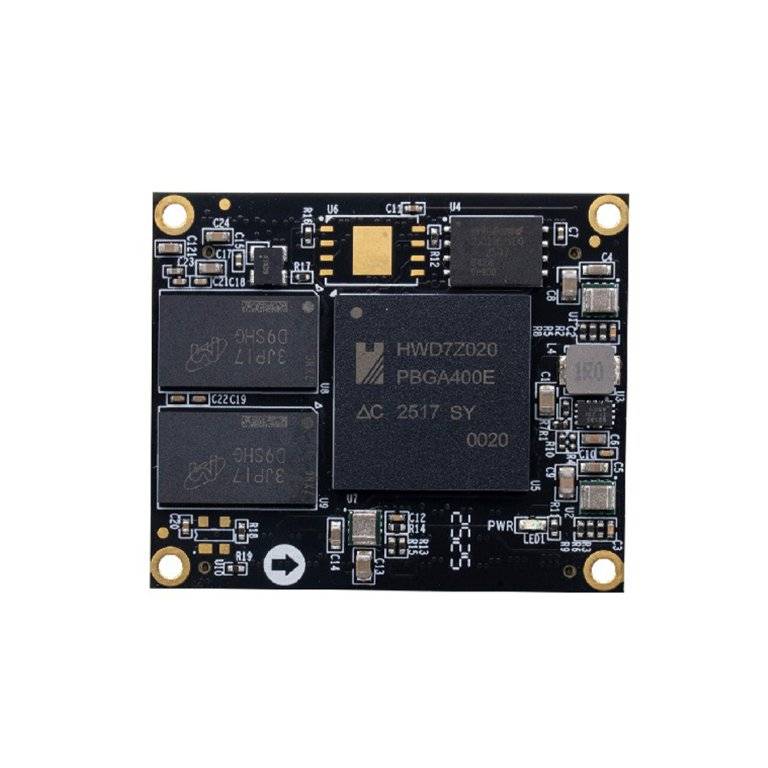
China FPGA Zynq SoC SoM – PBC7Z020G
China FPGA Zynq SoC SoM · dual-core A9 + FPGA heterogeneous · -55~125°C high-reliability wide temperature · 35×42mm ultra-compact
$122.92Tax not included View details →
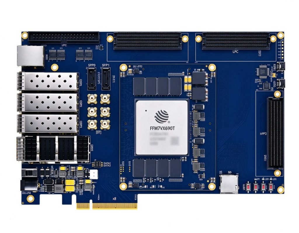
The DUF7690T development board is based on the Fudan Micro JFM7VX690T36-2FFG1761I industrial-grade FPGA (Vivado toolchain compatible), integrating 693K logic cells, 108K LUTs, 3,600 DSP slices and 52.9 Mb of Block RAM, with 36 GTH transceiver pairs (up to 10.3 Gbps per channel) and a PCIe 3.0 x8 hard core. The 100×80mm SOM integrates 4GB DDR3 (2×2GB/64-bit) and dual QSPI + BPI boot; the 220×130mm carrier board breaks out 2×FMC HPC + 1×FMC LPC, 3×SFP+, 1×QSFP (40G), Gigabit Ethernet, SATA, SD card and USB-JTAG, with 200MHz + 125MHz + 156.25MHz differential clocks. Typical applications: for software-defined radio (SDR), pair it with AD9361/AD9371 FMC daughter cards for JSR-standard waveforms, 5G small cells and satellite ground station localization; for radar signal processing, the 3,600 DSPs + 36 GTHs support pulse compression, beamforming, DBF and SAR imaging front-ends; for high-speed data acquisition, FMC HPC connects directly to AD9680/AD9152 ultra-high-speed ADCs/DACs with PCIe 3.0 x8 host backhaul; for video & image processing, aggregate multi-channel SFP+ video streams, 8K video stitching and FPGA hardware encode/decode preprocessing; for high-speed communication prototyping, use QSFP 40G + Aurora protocol stacks for 10G/40G optical communication, OTN and CPRI fronthaul prototyping. The JFM7 series is Vivado-compatible with an industrial -40~85℃ range, and can replace the XC7VX690T in high-reliability equipment localization projects. The SOM + carrier board ships as a complete assembly, with optional FMC ADC/DAC and SDR daughter cards; final configuration is subject to commercial confirmation. Reference price from $3,846, supporting volume orders and localization customization.
Interface, cooling, structure and batch supply can be customized per project · we respond within 1 business day after submission.
The DUF7690T development board is based on the Fudan Micro JFM7VX690T36-2FFG1761I industrial-grade FPGA (Vivado toolchain compatible), integrating 693K logic cells, 108K LUTs, 3,600 DSP slices and 52.9 Mb of Block RAM, with 36 GTH transceiver pairs (up to 10.3 Gbps per channel) and a PCIe 3.0 x8 hard core. The 100×80mm SOM integrates 4GB DDR3 (2×2GB/64-bit) and dual QSPI + BPI boot; the 220×130mm carrier board breaks out 2×FMC HPC + 1×FMC LPC, 3×SFP+, 1×QSFP (40G), Gigabit Ethernet, SATA, SD card and USB-JTAG, with 200MHz + 125MHz + 156.25MHz differential clocks.
Typical applications: for software-defined radio (SDR), pair it with AD9361/AD9371 FMC daughter cards for JSR-standard waveforms, 5G small cells and satellite ground station localization; for radar signal processing, the 3,600 DSPs + 36 GTHs support pulse compression, beamforming, DBF and SAR imaging front-ends; for high-speed data acquisition, FMC HPC connects directly to AD9680/AD9152 ultra-high-speed ADCs/DACs with PCIe 3.0 x8 host backhaul; for video & image processing, aggregate multi-channel SFP+ video streams, 8K video stitching and FPGA hardware encode/decode preprocessing; for high-speed communication prototyping, use QSFP 40G + Aurora protocol stacks for 10G/40G optical communication, OTN and CPRI fronthaul prototyping. The JFM7 series is Vivado-compatible with an industrial -40~85℃ range, and can replace the XC7VX690T in high-reliability equipment localization projects.
The SOM + carrier board ships as a complete assembly, with optional FMC ADC/DAC and SDR daughter cards; final configuration is subject to commercial confirmation. Reference price from $3,846, supporting volume orders and localization customization.
| Parameter | Specification |
|---|---|
| Product Model | DUF7690T V1.0 |
| FPGA Chip | Fudan Micro JFM7VX690T36-2FFG1761I (Vivado toolchain compatible) |
| Speed Grade / Temperature | -2 speed grade · Industrial -40℃ ~ 85℃ |
| Logic Cells / LUTs | 693K Logic Cells · 108K LUTs |
| DSP / Block RAM | 3,600 DSP Slices · 52.9 Mb Total Block RAM |
| GTH Transceivers | 36 TX/RX pairs, up to 10.3 Gbps per channel |
| PCI Express | 1 hard core PCIe Gen3 x8 (8.0 GT/s) |
| User I/O | 528 single-ended / 264 differential pairs (1.2V / 1.8V adjustable, 1.8V default) |
| On-board Memory | 4GB DDR3 (2 × 2GB / 64-bit, up to 1866 Mbps) |
| Boot Options | JTAG · QSPI · BPI (DIP switch selectable) |
| On-board Clocks | 1×200MHz differential oscillator (FPGA) + 1×125MHz + 1×156.25MHz differential oscillators (GTH reference) |
| FMC Interfaces | 2 × FMC HPC (8 GTH pairs, 168 I/O) + 1 × FMC LPC (1 GTH pair, 72 I/O) |
| Optical Interfaces | 3 × SFP+ · 1 × QSFP (40G) |
| Other Interfaces | 1 × Gigabit Ethernet · SATA · SD card · USB-JTAG · UART · 2 user LEDs + 2 buttons · 40P expansion header |
| SOM Structure | 100 × 80 mm · all I/O via board-to-board connectors |
| Carrier Structure | 220 × 130 mm · immersion gold process |
| Power Supply | +12V / 3A DC input |
5G/6G base stations and high-speed network equipment impose strict requirements on protocol processing, data forwarding and deterministic latency. With high-speed transceivers, reconfigurable protocol stacks and parallel pipelines, FPGA powers 100G optical communication, protocol processing and network security acceleration, providing a high-throughput, low-latency hardware platform from R&D to mass production.
From university labs to enterprise pre-research, rapidly verifying algorithms and hardware architectures is the critical first step to project success. Duyuan FPGA development boards and SoMs provide rich high-speed interfaces, complete reference designs and end-to-end technical support for ASIC prototype verification, high-speed data acquisition, instrument development and academic research — helping teams turn ideas into working hardware systems quickly.
4K/8K video, machine vision and industrial cameras impose strict requirements on end-to-end latency and interface coverage. With hardware-direct video paths and parallel pipelines, FPGA delivers microsecond-level deterministic processing in video encoding/decoding, image pre-processing, multi-protocol interfaces and low-latency transport, supporting deep customization of video services and vision algorithms.
Phased-array and imaging radar impose strict requirements on signal processing platforms: multi-channel parallel acquisition, high-throughput dataflow and deterministic low latency. With its reconfigurable parallel architecture, FPGA serves as the core carrier of radar signal processing, delivering multi-channel parallel, high-throughput, deterministic low-latency compute in beamforming, pulse compression and target detection, while supporting algorithm reconfiguration and platform evolution.
China FPGA
China FPGA Zynq SoC SoM · dual-core A9 + FPGA heterogeneous · -55~125°C high-reliability wide temperature · 35×42mm ultra-compact
 China FPGA
 China FPGA
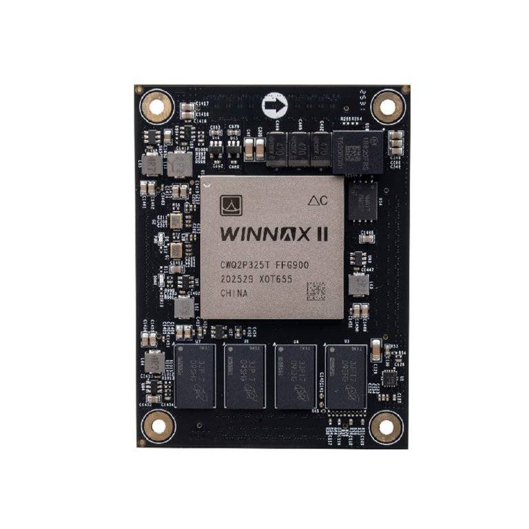
China FPGA industrial-grade SoM · CWQ2P325T · 326K logic · 16 GTX · 2GB DDR3
We respond within 1 business day after submission, supporting selection consulting, parameter customization and batch supply.
Contact · +86 18621324348