Building High-Speed Data Acquisition Cards with FPGA: Why FMC HPC + PCIe x8 Is the Golden Combination
Oscilloscopes, digitizers, phased-array radars, software-defined radios and high-speed vibration monitoring — the core of all these systems is “high-speed ADC sampling → data packing → transfer to the host for processing.” Why must this step use an FPGA rather than an MCU, a DSP or a CPU sampling directly? Why have the FMC HPC connector and the PCIe x8 interface become the golden combination for high-speed acquisition cards? This article starts from a real 250MSPS acquisition project.
1. Why High-Speed Acquisition Demands an FPGA
Let’s start with the numbers. A typical high-speed ADC such as the AD9643: 14-bit, 250 MSPS, dual channel. Converting to data rate:
Dual-channel 14-bit @ 250 MSPS
= 2 ch × 14 bit × 250 MS/s
= 7.0 Gbps raw data rate
= 875 MB/s continuous data stream
That means every second 875MB of sampled data must be moved from the ADC to host memory. If any link in the chain cannot keep up, samples are lost:
- MCU / ARM: SPI/parallel ports top out at 50MB/s, 17× short — samples lost immediately
- DSP: DMA ports top out at 200MB/s, 4× short — samples lost when the buffer fills
- CPU reading GPIO directly: OS scheduling latency makes a single read cycle 10μs-class — like catching a waterfall with a bucket
The value of the FPGA: it is a parallel, deterministic hardware circuit. The ADC’s LVDS data stream comes in, and the FPGA uses IDDR primitives to receive 8 differential pairs on every clock edge, performing deserialization, alignment, timestamping, FIFO buffering, and then bulk-transferring data into the host via PCIe DMA. The entire chain has no OS scheduling, no cache misses, no interrupt latency — clock cycles are deterministic.
That is why the control core of every industrial high-speed acquisition card, oscilloscope and digitizer is an FPGA — not because the FPGA is smarter than a CPU, but because it is fast, deterministic and parallel enough.
2. Standard Architecture of a High-Speed Acquisition Card
The complete data path looks like this:
Analog signal ───▶ High-speed ADC (FMC daughter card) → LVDS / JESD204B → FPGA logic (deserialization / alignment / trigger / decimation / FIFO) → DDR3 buffer (burst capture, underrun cushion) → PCIe 2.0 x8 DMA → Host memory → Host software
There are four critical bottlenecks on this path, and each one determines the real performance of the acquisition card:
1. Physical Link from ADC to FPGA: FMC HPC
High-speed ADC daughter cards are not soldered directly onto the main board — they are built as standard FMC (FPGA Mezzanine Card) daughter cards. The FMC HPC connector provides:
- 8 GTX high-speed serial pairs (up to 6.6 Gbps, for JESD204B)
- 168 single-ended/differential IOs (for LVDS parallel ADCs)
- Dedicated clock, trigger and GA signal pins
- High-current power pins (the daughter card powers itself)
One FMC HPC slot can host an AD9643 (250MSPS ADC), AD9152 (DAC), AD9361 (software-defined radio), FT601 (USB3.0) or even an FMC-to-40G optical module. That is why we insist on HPC instead of LPC — LPC has only 10 differential IO pairs and no GTX, so it cannot connect a high-speed ADC at all.
2. On-Board Buffering: DDR3 Is Not Optional
The ADC continuously outputs 875MB/s, while PCIe 2.0 x8 has a theoretical bandwidth of 4GB/s — PCIe looks fast enough. But in a real system the host always has bursts: OS scheduling, host software processing, disk I/O. Without DDR3 buffering, those bursts turn directly into lost samples.
The 4GB DDR3 acts as an “elastic reservoir” on this path: whatever the ADC sends is accepted and written into DDR3 first, and PCIe DMA moves it out in bulk whenever the host is free. For a 1-second one-shot burst capture, 875MB of data can be stored completely in DDR3 without losing a single sample. With 2GB DDR3, continuous capture time is halved.
3. FPGA-to-Host Transfer: The Real Difference Between PCIe x8 and x2
This is the most easily overlooked point. Many FPGA development boards expose only PCIe x2 — it looks like “there is PCIe, that’s enough”, but the real bandwidth differs by 4×:
| PCIe Configuration | Theoretical Bandwidth | Usable (8B/10B encoding + protocol overhead) | Sustainable Acquisition Rate |
|---|---|---|---|
| PCIe 2.0 x2 | 1.0 GB/s | ~700 MB/s | Cannot sustain 14-bit dual-channel 250MSPS — samples lost |
| PCIe 2.0 x4 | 2.0 GB/s | ~1.5 GB/s | Marginal for single-channel 250MSPS |
| PCIe 2.0 x8 | 4.0 GB/s | ~3.0 GB/s | Ample headroom for dual-channel 250MSPS + multi-channel triggering |
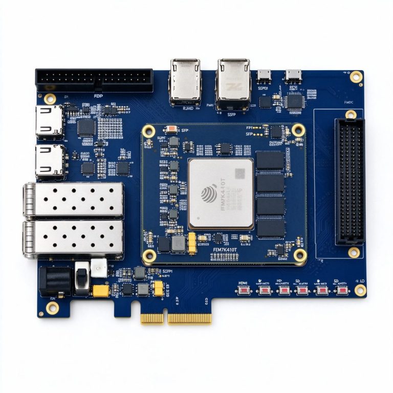
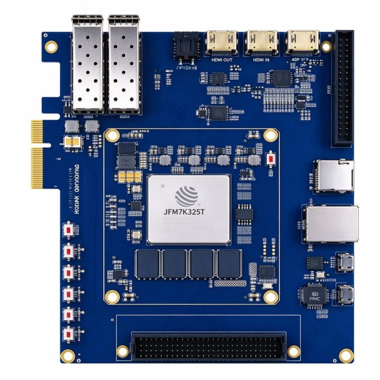
That is why Duyuan’s DUK7325T / DUK7410T both implement PCIe at x8 — the third-party original board exposes only x2; not because the chip does not support it, but because the design saved cost. The Kintex-7 PCIe block is Gen2 x8 in hardware; it only takes 4 more differential pairs on the PCB. For acquisition customers, the difference between x2 and x8 is not “a little faster” — it is whether the ADC sampling rate can be sustained at all.
4. Clock Synchronization: Why the 125MHz Differential Oscillator Matters
High-speed acquisition is extremely sensitive to clock jitter. The jitter of the ADC sampling clock directly determines the signal-to-noise ratio — a 250MSPS ADC requires sampling clock jitter < 1ps. The on-board 125MHz differential oscillator is dedicated to the GTX transceivers, and the 200MHz differential oscillator serves the FPGA logic; the two clock domains are kept separate to avoid mutual contamination. For JESD204B synchronized acquisition, this clock quality directly affects multi-channel phase consistency.
3. A Real-World Case: Building a 250MSPS Acquisition Prototype with DUK7410T
Duyuan Electronics recently helped a customer build a prototype: a high-speed digitizer based on DUK7410T + a third-party FMC-ADC9643 daughter card (AD9643, dual-channel 14-bit 250MSPS).
DUK7410T + FMC AD9643 + Host Software
- FPGA: JFM7K410T, 406K LC / 1,540 DSP / 28.6 Mb BRAM
- ADC: FMC daughter card AD9643, dual-channel 14-bit 250MSPS
- Buffering: on-board 4GB DDR3
- Transfer: PCIe 2.0 x8 DMA, measured 2.6 GB/s
- Triggering: FPGA hardware trigger (rising/falling edge, window), latency < 50ns
Measured result: dual-channel continuous capture for 1 second — 875MB written completely into DDR3, then moved to the host over PCIe x8, with 0 samples lost. With the third-party original board’s PCIe x2, continuous capture in the same configuration starts losing samples after 0.6 seconds — that is the real gap between x8 and x2.
After this prototype was verified, the customer built their own carrier board around DUK7410T’s core board (83.8×64.8mm), replaced the FMC slot with an ADC soldered directly onto the board, replaced the PCIe connector with a gold-finger edge, and turned it into a production acquisition card 6 months later.
4. Choosing Among Duyuan’s Three Boards for Acquisition
Not every acquisition project needs a Virtex-7. Choose by sampling rate and channel count:
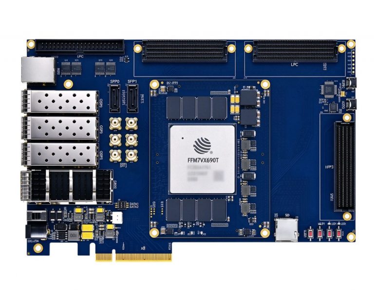
| Scenario | DUK7325T $1,231 | DUK7410T $1,538 | DUF7690T $3,846 |
|---|---|---|---|
| ADC sampling rate | ≤ 125 MSPS | ≤ 250 MSPS | ≥ 500 MSPS |
| ADC channels | 2 channels | 2–4 channels | 8+ channels |
| DSP demand | Simple decimation/FIR | Real-time FIR/FFT | Pulse compression/MIMO radar |
| Optical sync | 2×SFP+ | 2×SFP+ | QSFP 40G + 3×FMC |
| Typical use | Vibration monitoring, industrial acquisition | Digitizers, SDR prototyping | Phased-array radar, software-defined radio |
The selection principle is simple: first calculate the total ADC data rate, then the PCIe bandwidth headroom, and finally whether the DSP/BRAM is enough for real-time processing. For 80% of low- and mid-speed acquisition projects, DUK7325T is enough; for 250MSPS dual-channel or simple real-time FFT, move up to DUK7410T; only for hard cases like radar, ultra-wideband SDR and multi-channel synchronization do you need DUF7690T’s 36 GTH pairs and 3 FMC slots.
The essence of high-speed acquisition is not “how fast you sample”, but “no link in the entire chain fails”. Fast enough ADC, parallel enough FPGA, large enough DDR3, wide enough PCIe, stable enough clock — skimp on any link and it eventually becomes lost samples on the screen. FMC HPC + PCIe x8 + 4GB DDR3 is the minimum reliable configuration we put together for customers on this path.