Real-Time Industrial Vision Inspection with FPGA: From GigE Cameras to Defect Calibration
Along a production-line defect inspection pipeline, from camera pixels to the rejection signal, where exactly is the FPGA irreplaceable? This article first tallies the bandwidth budget of the full data flow, then breaks down the four roles FPGA plays in the vision pipeline, compares the real-time limits of traditional algorithms versus deep learning, and finally gives a deployable hardware selection through a real PCB solder-joint AOI station case.
1. First, the Bandwidth Bill: Data Flow on a 1080p60 Line
The first hurdle in industrial vision is not algorithms, it is bandwidth. Start with the most ordinary line path—a single 1080p, 60fps GigE Vision camera—and compute its data rate:
| Output format | Calculation | Result | Can it ride a gigabit link? |
|---|---|---|---|
| 8-bit Bayer (most common) | 1920 × 1080 × 8 bit × 60 | ≈ 995 Mb/s ≈ 124 MB/s | Saturates 99.5% of 1 Gbps, barely |
| 12-bit Bayer (HDR/low light) | 1920 × 1080 × 12 bit × 60 | ≈ 1.49 Gb/s ≈ 187 MB/s | Exceeds gigabit; needs 2.5G/10G or CoaXPress |
| 4 × 8-bit cameras | 995 Mb/s × 4 | ≈ 4 Gb/s ≈ 500 MB/s | Needs 4× gigabit aggregation or 10G uplink |
If you stream these raw frames whole to a CPU or GPU, every channel is shoving 124–187 MB per second; four channels mean 500 MB/s. On the CPU side you still have to process a full frame—burning bandwidth and compute at both ends. What defect detection actually needs is only “where is the anomaly, what type, what coordinates”—often just a few hundred bytes.
The Key: Where Pixels Are Processed Decides the Cost of the Whole Pipeline
Moving raw frames elsewhere and processing them is the “mover” mindset; processing pixels in place as they flow is the “pipeline” mindset. The first adds a full channel of bandwidth and compute for every extra camera; the second adds only processing logic.
2. The Four Roles of FPGA in the Vision Pipeline
Role 1: Interface Bring-Up and Multi-Camera Synchronization
GigE Vision / CoaXPress protocol parsing, camera parameter configuration, and trigger management are handled directly by the FPGA’s MAC layer and trigger logic. Multiple cameras lock to the same hardware trigger clock, guaranteeing that frames from different viewpoints are exposed at the same instant—something software struggles to match deterministically.
Role 2: Image Preprocessing (Denoising, Gain, Bayer Interpolation)
Denoising, white balance, gain, Bayer interpolation, ROI extraction—all are per-pixel operations. The FPGA pipeline naturally advances one pixel per clock cycle; the 1080p60 pixel clock is around 148.5 MHz, well within the timing margin of devices like the JFM7K410T. The same per-pixel work on CPU is a loop of several to tens of milliseconds per frame; on FPGA it is a fixed latency of a few dozen clock cycles.
Role 3: Defect Detection (Template, Difference, Connected Components)
Template matching, frame differencing, thresholding, connected-component analysis, morphological processing—all parallel, all pipelinable. Template matching on a 1080p image on FPGA runs in under 1 ms per frame, with latency independent of frame rate and fully deterministic—a hard requirement for line cycle time.
Role 4: Result Output and IO Coordination
The verdict directly drives the rejection actuator, alarm lamp, and statistical counters. FPGA GPIO output latency is nanosecond-scale, with no detour through OS, driver, or application layer. The instant a defect appears, the rejection signal has already reached the actuator.
3. Two Algorithm Paths: Traditional Vision vs Deep Learning
“Just add deep learning” has become a mantra on vision projects in recent years, but the real-time boundary between the two paths must be drawn clearly:
| Dimension | Traditional vision (template/difference/morphology) | Deep learning (CNN/YOLO-class) |
|---|---|---|
| 1080p single-frame latency | <1 ms (FPGA pipeline) | 2–10 ms (GPU) or higher (general NPU) |
| Resource footprint | Small LUT/DSP count | Heavy DSP + external memory bandwidth |
| Interpretability | Adjustable thresholds, traceable defects | Black box, hard to localize false positives |
| Best fit | Fixed defect patterns, fast cycle lines | Complex defects, offline re-inspection of varied samples |
| Implemented on FPGA | Mature, highly engineered | Needs quantization/pruning; usually on CPU/GPU |
The mainstream 2026 line architecture is FPGA preprocessing + traditional real-time verdict + deep learning offline re-check: FPGA guarantees the verdict and rejection within cycle time, while deep learning performs secondary confirmation on suspicious regions—each doing what it does best.
4. A Real Case: PCB Solder-Joint AOI Station
Engineering Case · 01: SMT Line Solder-Joint Inspection—60 fps Continuous, False-Call Rate < 0.5%
An SMT line AOI station must detect cold solder joints, solder bridges, and missing components, run continuously at 60 fps, with a false-call target below 0.5% and cold-joint miss rate below 1%.
- Cameras: 2 × GigE 20 MP industrial cameras, actually cropped to 1080p ROI, 8-bit Bayer output
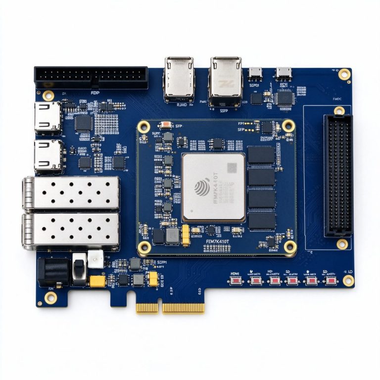
- Board: DUK7410T (Fudan Micro JFM7K410T, 406K logic cells, FMC HPC, 4 GB DDR3)
- Data flow: 2 × 995 Mb/s ≈ 2.5 Gb/s into FPGA → DDR frame buffer → template differencing + connected-component analysis → verdict output
Measured results: single-frame processing < 0.8 ms; end-to-end latency from camera trigger to rejection output < 1.5 ms; false-call rate < 0.5%; cold-joint detection rate > 99%.
Versus CPU baseline: end-to-end latency dropped from ~15 ms to < 1.5 ms, host CPU load from 85% to 5%—the original software pipeline could only reach 30 fps; switching to FPGA doubled throughput.
The key to this station is not a fancy algorithm—it is that the inspection action keeps up with the line cycle. The moment a defect frame arrives, the verdict and rejection must complete before the next frame.
5. How to Select Hardware: Three Boards, Three Strategies
Selection follows three questions: how many cameras? how hard is the latency requirement? what is the total machine budget? Here are Duyuante’s three common platforms:
DUK7410T (¥9,999)—the Mid-Range Workhorse, Standard Choice for 1/2-Camera AOI
Fudan Micro JFM7K410T, 406K logic cells, 1,540 DSPs, FMC HPC, HDMI 4K input, 2× SFP+. FMC HPC connects directly to high-speed camera or ADC mezzanines; HDMI 4K input can double as display loopback. Vision positioning, defect detection, multi-channel stitching prototypes—most projects start here.
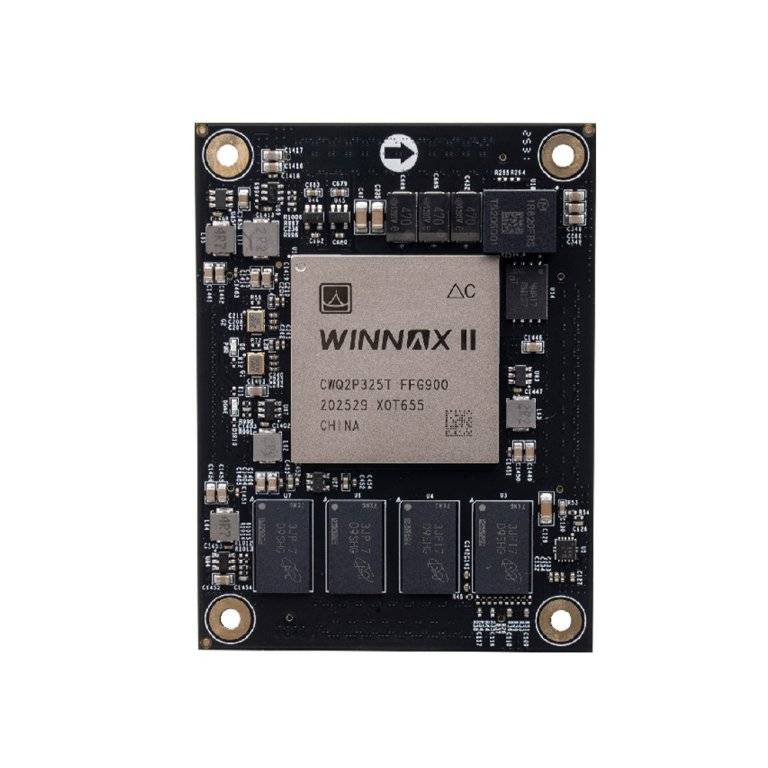
PBC7K325G (¥1,999)—Cost-Sensitive Embedded Machine Integration
China Kintex-7 architecture SoM, 326K logic, 16 GTX transceivers, 2 GB DDR3, industrial grade −40 to 85 °C. Single-camera fixed-pattern embedded inspection, or combined vision + motion-control controllers. Cost-sensitive products ship from here.
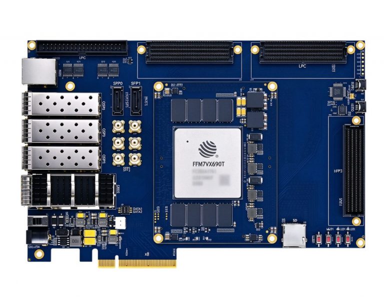
DUF7690T (¥24,999)—Multi-Camera Arrays and High-Performance Composite Systems
Fudan Micro JFM7VX690T, 693K logic cells, 3,600 DSPs, 36 GTH pairs, QSFP 40G. 8+ camera arrays, 8K stitching, or vision + fiber-communication composite systems—when you need big logic and big bandwidth, step up to this board.
The first principle of industrial vision is “don’t shuttle whole frames around”—process pixels where they flow through, and latency, bandwidth, and power problems disappear at once.
>
— Duyuante R&D Team