VU13P in Quantitative Trading: A Low-Latency Hardware Platform from Market Data Decoding to Order Execution
The essence of quantitative trading is completing the information loop of “market data arrival → signal computation → order transmission” in the shortest possible time. This article uses the AMD Virtex UltraScale+ XCVU13P (VU13P) platform as the main thread, explaining why it fits quantitative trading and how to deploy it into a deliverable low-latency trading chain.
The essence of quantitative trading is completing the information loop of “market data arrival — signal computation — order transmission” in the shortest possible time. On the microsecond timescale of an exchange matching engine, latency itself is cost: being one microsecond late means price slippage, lost opportunities, or the failure of an entire strategy. Over the past decade, leading proprietary trading firms have progressively migrated the most critical parts of the chain from CPU software to FPGA hardware — market data decoding on the card, order book on the card, strategy decisions on the card, and order generation on the card. This article uses the AMD Virtex UltraScale+ XCVU13P (VU13P) platform as the main thread, discussing why it fits quantitative trading and how to deploy it into a deliverable low-latency trading chain.
1. The Latency Structure of Quantitative Trading: Why the Answer Is FPGA
A typical automated trading chain — from a market data packet arriving at the NIC to an order leaving the NIC — passes sequentially through the network stack, market data parsing, order book maintenance, signal computation, risk checks, and order encoding. In a software stack, kernel interrupts, protocol stack processing, thread scheduling, and cache misses all introduce uncontrollable jitter; hardware implementation turns these stages into a fixed pipeline depth with deterministic latency, no interrupts, and no scheduling. Rough end-to-end tick-to-trade latency for different implementation approaches:
Table: End-to-end tick-to-trade latency comparison (compiled from public sources)
| Implementation | Typical end-to-end latency |
|---|---|
| Ordinary software + kernel network stack | 10–100 µs |
| Kernel-bypass software (DPDK / Onload + core pinning) | 1–5 µs |
| Full FPGA chain (parsing → strategy → order) | 300 ns – 1 µs |
| FPGA pre-armed trigger (pattern match and send) | 30–100 ns |
| Layer-1 switch (pure fan-out / replication) | approx. 5 ns |
Three properties of FPGA determine this order-of-magnitude gap: parallelism — multiple market data feeds and strategy instances run simultaneously in hardware without contending; determinism — no interrupts or scheduling, each packet’s processing latency is fixed, which matters equally for risk control and audit; proximity — optical ports connect directly into the FPGA, bypassing PCIe and the protocol stack, decoding packets as they arrive. Public data from the industry confirms this: certain solutions advertise sub-100 ns round-trip tick-to-trade latency, AMD’s reference design with partners for CME achieves pre-armed trigger latency at the 25 ns level; a 2025 paper in *Computer Applications and Software* describing an OpenCL-based ultra-low-latency market data acceleration system achieved 678 ns minimum market data processing on an Alveo U50 with 38.4 Gbit/s throughput, roughly 12x performance improvement over the software approach.
2. VU13P Platform Capability Overview
VU13P belongs to the AMD Virtex UltraScale+ family and is a representative device at the “logic scale × high-speed interface” balance point. According to AMD official product documentation, its key specifications are:
Table: XCVU13P key specifications (source: AMD official Virtex UltraScale+ product page)
| Metric | XCVU13P specification |
|---|---|
| System Logic Cells | 3,780K (approx. 3.78 million logic cells) |
| DSP Slices | 12,288 |
| GTY high-speed transceivers | 128 pairs (up to 32.75 Gb/s per pair) |
| User I/O | 832 |
| Integrated high-speed interfaces | PCIe Gen3 x16, 100G Ethernet MAC, 150G Interlaken (in-die hard blocks) |
| DSP compute | up to approx. 38 TOP/s |
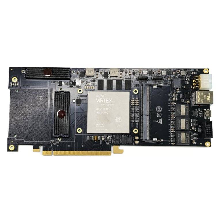
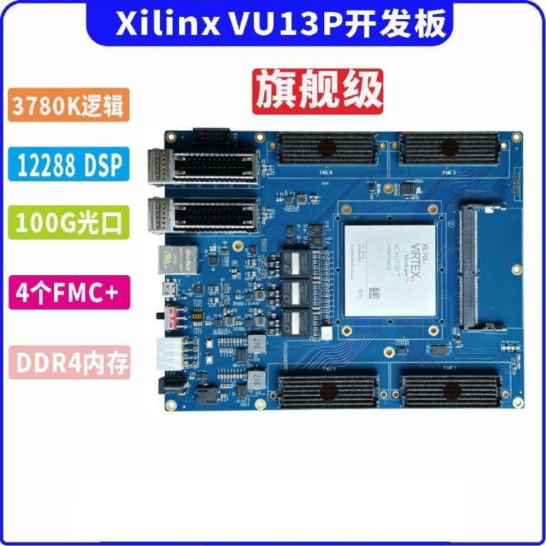
At the board level, Duyuan Electronics’ VU13P ultra-high-end development platform offers PCIe Gen3 x16 gold fingers, multiple 100G optical ports (QSFP28), FMC+ high-speed expansion, DDR4 SODIMM expansion, and an industrial-grade -40°C to 85°C temperature range. For quantitative trading, this board naturally provides three things: directly connecting multiple exchange feeds into the FPGA (optical ports + GTY), placing substantial strategy logic inside the FPGA (3.78 million logic cells + 12,288 DSP), and high-bandwidth bidirectional host interconnect (PCIe Gen3 x16).
3. Four Core Applications of VU13P in the Quantitative Trading Chain
3.1 Market Data Decoding and Preprocessing (Feed Handler)
Exchange market data protocols (NASDAQ ITCH, CME MDP3, the FAST format commonly used by European exchanges, etc.) arrive at extremely high packet rates; software parsing requires per-packet decoding, validation, and structure reconstruction, making it the earliest and most typical bottleneck in the chain. On VU13P, market data parsing is implemented as a hardware pipeline: packets are decoded as byte streams as they enter the optical port, with field extraction, validation, and protocol reassembly completed within fixed pipeline stages, while multiple feeds (multiple exchanges, A/B primary-backup lines) are processed in parallel. The 128 GTY transceivers and multiple 100G optical ports provide ample simultaneous connection capacity; for exchanges publishing via primary-backup dual lines (such as CME’s A/B lines), line arbitration and seamless failover can be implemented in hardware to avoid market data gaps caused by single-line jitter. The parsed standard market data structures are written directly into on-chip storage for downstream strategy modules, never passing through the host CPU.
3.2 Hardware Order Book and Parallel Strategy Execution
Maintaining a queryable order book requires frequent insert, delete, modify, and sort operations; software implementations rely on memory access and locks, while hardware implementations map price levels directly onto on-chip Block RAM structures, with price lookup and matching decisions completed in fixed cycles. On this basis, VU13P’s 3.78 million logic cells allow multiple strategy instances to run in parallel on a single device: different instruments, different markets, and even different strategy logic (market making, cross-market arbitrage, latency arbitrage, statistical regression) can occupy independent logic partitions, sharing the same parsed market data stream without interference. For latency-sensitive trigger strategies, a “pre-armed order” approach can be used: order templates are written into the transmit buffer in advance, and when hardware detects the set condition (price breakthrough, volume ratio change) it triggers transmission directly, bypassing the software decision path, compressing latency to tens of nanoseconds.
3.3 Pre-Trade Risk
Exchanges and compliance frameworks impose increasingly strict risk requirements on algorithmic trading: price bandwidth, per-order quantity caps, cumulative daily position, order frequency, and other checks must complete before an order is sent. The problem with software risk checking is that it sits on the critical path and adds latency; FPGA risk checking places check logic in parallel alongside the order path — every order passes through several risk check stages in the hardware pipeline, and is immediately encoded and sent on approval, or blocked in nanoseconds on rejection. Risk rules are configured via registers/memory tables and can be hot-updated within the trading day, satisfying compliance requirements without sacrificing low latency on the main path.
3.4 Backtesting, Simulation, and R&D Acceleration
Beyond the production chain, VU13P’s large logic resources also support strategy R&D: load market data replay and simulation engines on the development board for hardware-level backtesting against historical data, running multiple strategies in parallel — significantly faster than software simulation; use Vivado/Vitis HLS to quickly map C/C++ algorithms to hardware implementations, shortening the “strategy idea → testable hardware” iteration cycle. A typical engineering organization is “FPGA runs the production path, CPU runs monitoring and analytics”: production order and market data processing happen entirely on the card, while the host reads status via PCIe Gen3 x16 and pushes down strategy parameters and risk rules, balancing performance and operations.
4. Typical End-to-End System Architecture
A VU13P-based quantitative trading platform has a typical topology as follows:
- Market data ingress: exchange feeds enter the FPGA directly via 100G optical ports (QSFP28), with 128 GTY pairs carrying multiple lines;
- Hardware parsing: Feed Handler modules decode, validate, and arbitrate A/B lines in a pipeline according to protocol (ITCH/FAST/MDP3, etc.);
- Order book and signals: on-chip BRAM maintains order books for multiple instruments, strategy partitions compute signals in parallel, and orders are generated when trigger conditions are met;
- Risk and encoding: orders pass pre-trade risk checks and are encoded into exchange protocol messages before entering the transmit buffer;
- Host interconnect: order acknowledgements, fill reports, and status monitoring are sent to the host via PCIe Gen3 x16; strategy parameters and risk rules are pushed down from the host;
- Expansion interfaces: FMC+ is used to connect custom NICs/accelerator daughter cards, OCULINK for board-to-board high-speed interconnect for multi-board scaling.
In deployment form, the VU13P development board can serve directly as a PCIe accelerator card inside a server; for rack-space and power-sensitive scenarios, a lower-power core board form factor can be customized based on this platform.
5. Engineering Advantages of VU13P over Other Approaches
Table: Quantitative trading hardware platform comparison perspective
| Dimension | VU13P (FPGA) relative advantage |
|---|---|
| End-to-end latency | full chain 300ns–1µs, pre-trigger 30–100ns; software approaches typically 1–100µs |
| Latency determinism | fixed pipeline depth, no interrupt/scheduling jitter, good for risk and audit |
| Parallel capacity | 3,780K logic cells + 12,288 DSP, multiple strategies/instruments simultaneously |
| Interface bandwidth | 128×GTY, multiple 100G optical ports, PCIe Gen3 x16, direct multi-exchange feed |
| Flexibility | reconfigurable: strategy changes are config/reload, no board replacement; much shorter development cycle than ASIC |
| Development threshold | lower than ASIC; Vitis HLS/OpenCL maps from C/C++, key paths further optimized in RTL |
Compared with CPU: VU13P is an order of magnitude ahead in latency and determinism; compared with GPU: GPUs excel at batch throughput but the pipeline and scheduling introduce latency jitter that makes them unsuitable for nanosecond-critical paths, while VU13P’s deterministic latency is a natural fit; compared with ASIC: ASIC has the best performance but prohibitive one-time cost and development cycle, suitable only for fully frozen algorithms, whereas VU13P retains flexibility for strategy evolution. This is why proprietary trading firms widely adopt “FPGA for the critical path, CPU/GPU for research and offline computation” as the standard division of labor.
6. Development and Deployment Essentials
- Toolchain division: critical paths (protocol parsing, order encoding) use RTL to guarantee latency; strategy logic can be quickly implemented with Vitis HLS / OpenCL, validating behavior in software simulation first, then synthesizing to hardware;
- Modular interfaces: Feed Handler, Order Book, Strategy, Risk, and Gateway uniformly use AXI-Stream data interfaces, making replacement, reuse, and team collaboration easier;
- Clock and synchronization: in multi-board/multi-site deployments, introduce PTP/1PPS and a low-jitter clock tree to unify the time base, ensuring fill reports and market data timestamps align;
- Start from a standard board: first complete market data parsing and strategy validation on the VU13P development board, run the latency chain through, then customize the board form factor (interface count, power, mechanical structure) per project needs;
- Monitoring and regression: keep statistics counters and ILA observation points in the hardware logic, monitor per-stage pipeline latency during the trading day, and any degradation can be located quickly.
7. Limitations and Selection Recommendations
FPGA is not the answer for every quantitative scenario. If a strategy rebalances at minute or hour horizons, or relies on large-scale machine learning features with frequent iterations of complex models, the cost and flexibility advantages of the CPU/GPU software stack are more obvious; if the team lacks hardware development capability, the evaluation, debugging, and maintenance cycle of an FPGA project needs full allowance. When hardware low latency is confirmed as a requirement, device selection can be layered by resource needs:
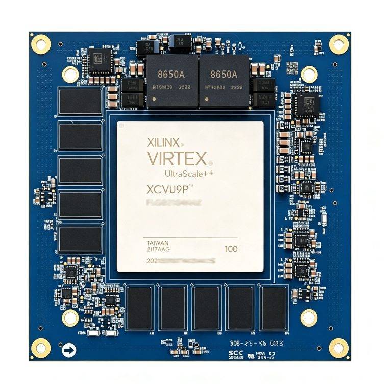
- VU9P: 2,586K logic cells, 6,840 DSP, with 2×200G + 4×100G optical ports, 32GB DDR4 ECC, PCIe x16 — suited to scenarios with large market data ingress and storage/bandwidth emphasis;
- VU13P: 3,780K logic cells, 12,288 DSP, 128×GTY — suited to parallel multi-strategy, complex strategy logic, and scenarios needing more on-chip resources; the comprehensive mainstay platform for this class of applications;
- VU13F: also 12,288 DSP, with 4×FMC+ providing extensive expandable I/O and daughter card interfaces — suited to system-level integration requiring custom NICs, RF front-ends, and other external hardware.
Note: latency figures in this article are typical ranges from public sources; actual values depend on protocols, packet rates, strategy implementation, and board routing. Selection and acceptance should be based on on-site measurement.
8. Conclusion
The hardware-ization of quantitative trading is a trend that has been certain for years: from the earliest NIC offload, to moving market data parsing and the entire order chain onto FPGA, to today where a single VU13P-class device simultaneously carries multi-market data, multi-strategy, and risk control. The value of VU13P lies in putting “scale” and “speed” on the same device — enough logic and DSP for complex strategy combinations to run in parallel in hardware, and enough GTY and 100G optical ports that multi-exchange ingress is no longer a bottleneck. Duyuan Electronics provides VU13P/VU9P standard development boards, custom core boards, market data decoding and low-latency chain IP packages, and end-to-end technical support, helping teams move quickly from evaluation-board validation to a deployable quantitative trading hardware platform.
References
- AMD, Virtex UltraScale+ FPGA product page (XCVU13P specifications): https://www.amd.com/en/products/adaptive-socs-and-fpgas/fpga/virtex-ultrascale-plus.html
- AMD/Xilinx with LDA, CME Tick-to-Trade 25 nanosecond reference solution: https://www.xilinx.com/publications/solution-briefs/partner/xilinx-lda-amd-tick-to-trade-solution-brief.pdf
- libfpga, FPGAs in high-frequency trading: the anatomy of a nanosecond (tick-to-trade latency comparison): https://libfpga.com/blog/fpgas-for-hft
- semidesignjobs, FPGAs in High-Frequency Trading: A Technical Deep Dive: https://www.semidesignjobs.com/blog/fpga-hft-technical-deep-dive
- Enyx, nxFramework (sub-100ns tick-to-trade platform): https://www.enyx.com/nxframework/
- Computer Applications and Software 2025, Design and implementation of an ultra-low-latency market data acceleration system based on OpenCL: https://shcas.net/cn/article/doi/10.3969/j.issn.1000-386x.2025.03.003
- ACM, DSL Programmable Engine for High Frequency Trading Acceleration (FAST protocol acceleration): https://dl.acm.org/doi/pdf/10.1145/2088256.2088268
Duyuan Electronics · Application Practice | Data as of September 2026; different institutions use different scopes, all sources annotated