Building a Wideband SDR Frontend: Signal Chain from ADC to FPGA
The core of Software Defined Radio (SDR): digitize the RF signal as early as possible, and leave the signal processing to the FPGA. A typical wideband SDR frontend chain is: antenna → LNA → mixer → ADC → FPGA (DDC + FFT + demodulation). Along this chain, FPGA transceiver bandwidth, DDR buffering, and DSP horsepower determine how wide an instantaneous bandwidth you can achieve.
1. SDR Frontend Signal Chain
A complete wideband SDR receive chain:
1. Antenna + RF frontend: receive over-the-air signals, amplify via LNA, band-pass filter.
2. Mixing / direct sampling: either down-convert to IF then sample, or direct RF sampling (wideband ADC sampling DC~6GHz).
3. ADC sampling: digitize the analog signal, output JESD204B serial data.
4. FPGA processing: receive JESD204B → DDC (digital down-conversion) → FFT / demodulation → upload to host via PCIe.
The FPGA does three things in this chain: catch high-speed serial data, perform real-time digital down-conversion, and transfer data to host via PCIe. These three tasks define the FPGA selection.
2. How to Calculate Instantaneous Bandwidth
The most critical SDR metric is Instantaneous Bandwidth (IBW) — the bandwidth the FPGA can process in real time after ADC sampling.
| Metric | Formula | Example (AD9680 14-bit 1GSPS) |
|---|---|---|
| ADC sample rate | f_s | 1 GSPS |
| Theoretical Nyquist bandwidth | f_s / 2 | 500 MHz |
| DDC output bandwidth | f_s / decimation | dec=4 → 125 MHz |
| JESD204B lane rate | f_s × 14 bit × frame overhead | ≈ 10.24 Gbps/lane |
| FPGA transceiver pairs | lanes per ADC | AD9680 → 4 lanes |
Bandwidth Budget Example
Project requirement: 100 MHz instantaneous bandwidth, dual-channel ADC.
- ADC: AD9680 (14-bit, 1 GSPS, JESD204B), 4 lanes per channel @ 10.24 Gbps.
- Dual ADC channels: need 8 transceiver pairs.
- Post-DDC data rate: 100 MHz × 2 ch × 16 bit (I/Q) = 3.2 GB/s.
- PCIe Gen2 x8 theoretical bandwidth ≈ 3.2 GB/s → fully loaded, need margin.
- Conclusion: choose DUK7410T (8× GTP + PCIe Gen2 x8) just barely fits, but requires DMA ping-pong buffering.
3. FPGA-side Resource Requirements
SDR frontend FPGA resource needs:
| Resource | Purpose | Typical Need (dual 100 MHz IBW) |
|---|---|---|
| High-speed transceivers | JESD204B RX + PCIe upload | 8 (ADC) + 4 (PCIe) = 12 pairs |
| DSP slice | DDC NCO + FIR filter + FFT | ~500~800 |
| BRAM | FIFO buffer + ping-pong | ~20~40 MB |
| DDR bandwidth | Large buffer + PCIe DMA | ≥ 5 GB/s |
| Logic cells | JESD204B IP + DDC + PCIe DMA | ~100K~150K LC |
4. Board Selection by Scenario
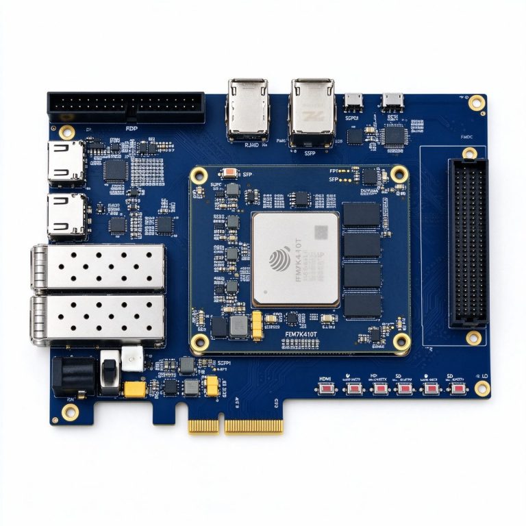
Entry: DUK7410T (¥9,999) — Single-channel 100 MHz SDR
8× GTP just fits one AD9680 mezzanine (4 lanes), remaining 4 pairs run PCIe Gen2 x8. 4GB DDR3 for ping-pong buffering. Suitable for education, single-channel spectrum monitoring.
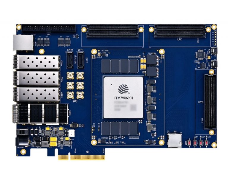
Mainstream: DUF7690T (¥24,999) — Dual-channel 200 MHz SDR
36× GTH @10.3G, dual FMC HPC for two ADC mezzanines. 3,600 DSP slices handle 8-channel DDC easily. PCIe Gen3 x8 doubles bandwidth. Suitable for wideband spectrum monitoring, electronic warfare prototypes.
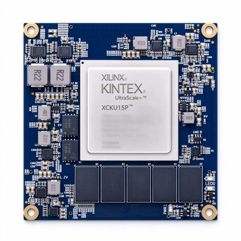
High-end: XCKU15P (¥15,999) — Direct RF Sampling SDR
GTY 28G transceivers support JESD204C lane rate 24Gbps. 8GB DDR4 ECC 19.2 GB/s. Suitable for direct RF sampling (6GHz ADC), multi-channel MIMO, phased array prototypes.
5. Three Common Pitfalls
Pitfall 1: JESD204B Lane Rate Exceeds Transceiver Limit
AD9680 at full 1 GSPS has lane rate ≈ 10.24 Gbps. DUK7410T GTP tops out at 6.6 Gbps — cannot connect! Must downsample to 250 MSPS (lane rate ≈ 2.5 Gbps). Or step up to DUF7690T (GTH @10.3G).
Pitfall 2: Insufficient DDR Bandwidth Causes Data Loss
Post-DDC 3.2 GB/s data must be written to DDR then read out via PCIe. DDR3 14.9 GB/s is theoretically enough, but actual read/write switching efficiency is only 60% — ≈ 9 GB/s. Calculate carefully for dual-channel; if insufficient, step up to DDR4.
Pitfall 3: Clock Misalignment, JESD204B Cannot Lock
JESD204B requires Device Clock + SYSREF alignment. ADC mezzanine clock must route through FMC CLK0 pin to FPGA MRCC/SRCC global clock inputs. If PCB routing is wrong, no matter how expensive the chip, it won’t work.
SDR frontend is not about buying the most expensive FPGA, but about getting the math right on ADC lane rate, instantaneous bandwidth, DDR buffering, and PCIe upload. Three calculations — transceiver pairs, DSP, DDR bandwidth — and the board choice falls out naturally.