
 FPGA SoM
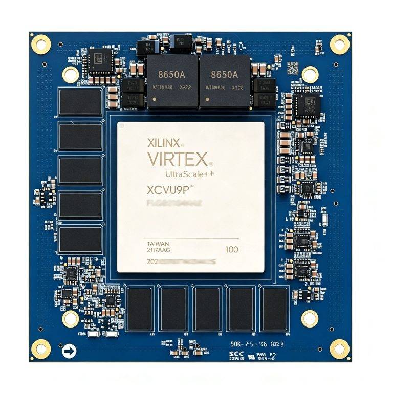
AMD Xilinx XCVU9P Virtex UltraScale+ FPGA Ultra High-Speed Fiber SoM
Virtex UltraScale+ flagship · fiber/PCIe high-speed interconnect · FMC expansion
$7,692.15Tax not included View details →
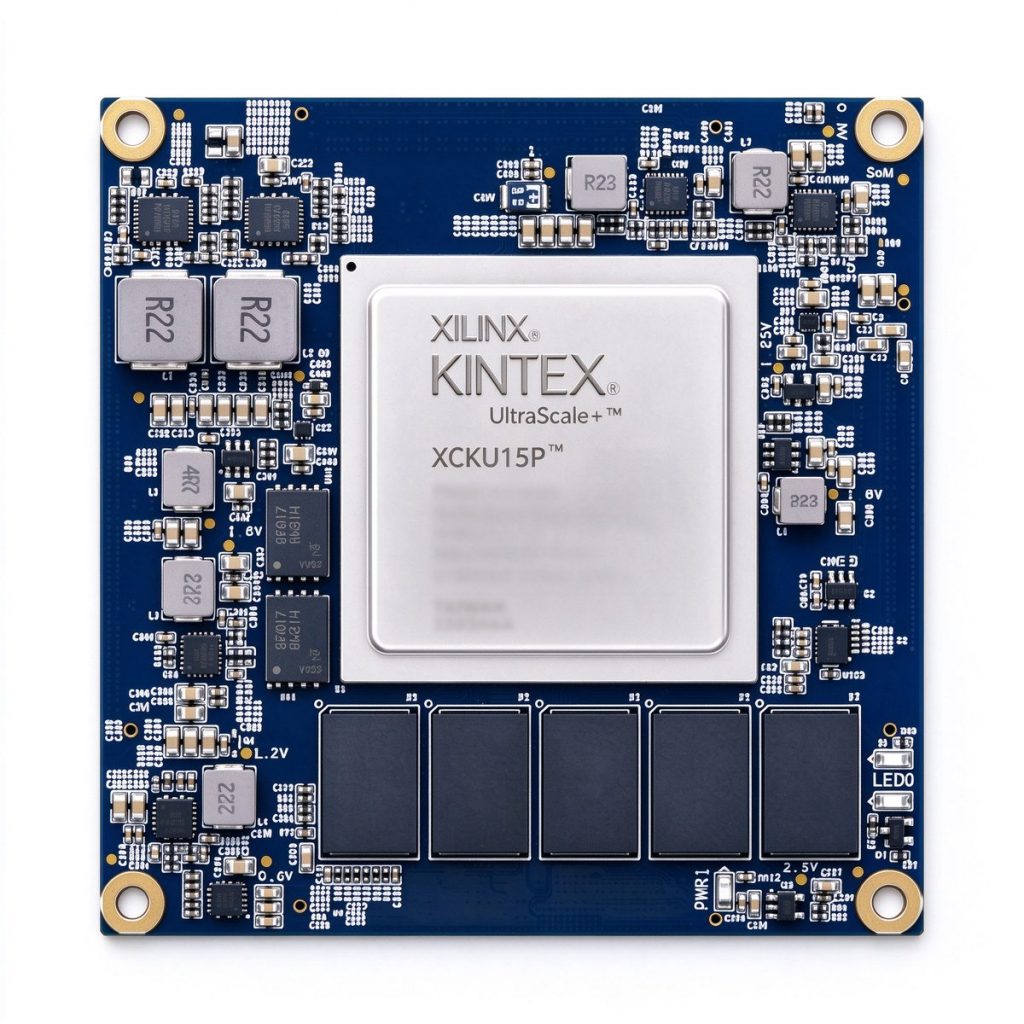
The DUKU15P SoM is built on the AMD Xilinx Kintex UltraScale+ XCKU15P-2FFVE1517I industrial-grade FPGA, integrating 1,143K logic cells, 523K LUTs, 1,968 DSP slices, 34.6 Mb Block RAM and 36 Mb UltraRAM. It carries 24 28.05 Gbps GTY transceivers and 32 16.3 Gbps GTH transceivers (56 in total), a PCIe Gen3 x16 hard core, four 150G Interlaken and four 100G Ethernet hard cores. The 80×80mm SoM uses an 18-layer PCB design and routes all 88 HD I/O pairs and 236 HP I/O pairs through four 240-pin board-to-board connectors, paired with 8GB DDR4 ECC, 256MB QSPI dual-backup Flash, a programmable low-jitter clock (
Interface, cooling, structure and batch supply can be customized per project · we respond within 1 business day after submission.
The DUKU15P SoM is built on the AMD Xilinx Kintex UltraScale+ XCKU15P-2FFVE1517I industrial-grade FPGA, integrating 1,143K logic cells, 523K LUTs, 1,968 DSP slices, 34.6 Mb Block RAM and 36 Mb UltraRAM. It carries 24 28.05 Gbps GTY transceivers and 32 16.3 Gbps GTH transceivers (56 in total), a PCIe Gen3 x16 hard core, four 150G Interlaken and four 100G Ethernet hard cores. The 80×80mm SoM uses an 18-layer PCB design and routes all 88 HD I/O pairs and 236 HP I/O pairs through four 240-pin board-to-board connectors, paired with 8GB DDR4 ECC, 256MB QSPI dual-backup Flash, a programmable low-jitter clock (<0.5 ps RMS) and PMBus power monitoring. It can be mounted directly onto your own carrier board for 100G networking, high-speed data acquisition, semiconductor ATE, radar signal processing and video & image processing scenarios. The SoM ships standalone; custom carrier boards (PCIe card, FMC carrier, 100G network carrier) are available. Final configuration is subject to commercial confirmation.
| Parameter | Specification |
|---|---|
| Product Model | DUKU15P V1.0 |
| FPGA Chip | AMD Xilinx Kintex UltraScale+ XCKU15P-2FFVE1517I |
| Speed Grade / Temperature | -2 speed grade · Industrial -40°C ~ 85°C |
| Package | FFVE1517 (FCBGA 45×45mm, 1517 pins) |
| System Logic Cells | 1,143K Logic Cells |
| CLB LUTs / Flip-Flops | 523K LUTs / 1,045K Flip-Flops |
| Block RAM / UltraRAM | 34.6 Mb Block RAM + 36 Mb UltraRAM |
| DSP Slices | 1,968 (27×18 multipliers) |
| Clock Management | 11 Clock Management Tiles (MMCM + PLL) |
| GTY Transceivers | 24 pairs, up to 28.05 Gbps per lane |
| GTH Transceivers | 32 pairs, up to 16.3 Gbps per lane |
| PCI Express | 1× PCIe Gen3 x16 hard IP (8.0 GT/s) |
| High-Speed Interface Hard IP | 4 × 150G Interlaken · 4 × 100G Ethernet |
| User I/O | 88 HD I/O pairs + 236 HP I/O pairs |
| On-board Memory | 8GB DDR4, 64-bit data bus + 8-bit ECC (×16 devices) |
| Configuration Flash | 256MB QSPI (A/B dual-backup boot) |
| Clock Source | On-board programmable low-jitter clock (<0.5 ps RMS) + 2 × 156.25 MHz low-jitter oscillators |
| Power Monitoring | TI INA226 PMBus current/voltage monitoring + LM75 on-board temperature sensor |
| Board-to-Board Connectors | 4 × 240-pin high-density connectors (four sides) |
| Power Supply | +12V via carrier; on-board multi-rail power tree (0.85V / 0.9V / 1.2V / 1.8V / 3.3V) |
| PCB Structure | 80 × 80 mm · 18-layer HDI · impedance controlled |
| Cooling | Bare SoM; heatsink/fan on carrier (optional by application) |
5G/6G base stations and high-speed network equipment impose strict requirements on protocol processing, data forwarding and deterministic latency. With high-speed transceivers, reconfigurable protocol stacks and parallel pipelines, FPGA powers 100G optical communication, protocol processing and network security acceleration, providing a high-throughput, low-latency hardware platform from R&D to mass production.
From university labs to enterprise pre-research, rapidly verifying algorithms and hardware architectures is the critical first step to project success. Duyuan FPGA development boards and SoMs provide rich high-speed interfaces, complete reference designs and end-to-end technical support for ASIC prototype verification, high-speed data acquisition, instrument development and academic research — helping teams turn ideas into working hardware systems quickly.
4K/8K video, machine vision and industrial cameras impose strict requirements on end-to-end latency and interface coverage. With hardware-direct video paths and parallel pipelines, FPGA delivers microsecond-level deterministic processing in video encoding/decoding, image pre-processing, multi-protocol interfaces and low-latency transport, supporting deep customization of video services and vision algorithms.
Phased-array and imaging radar impose strict requirements on signal processing platforms: multi-channel parallel acquisition, high-throughput dataflow and deterministic low latency. With its reconfigurable parallel architecture, FPGA serves as the core carrier of radar signal processing, delivering multi-channel parallel, high-throughput, deterministic low-latency compute in beamforming, pulse compression and target detection, while supporting algorithm reconfiguration and platform evolution.
FPGA SoM
Virtex UltraScale+ flagship · fiber/PCIe high-speed interconnect · FMC expansion
 FPGA SoM
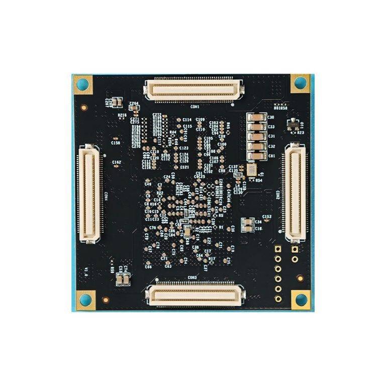
Artix-7 industrial-grade SoM · 215K logic · PCIe Gen2 · 1GB DDR3 · 180 I/O
 FPGA SoM
We respond within 1 business day after submission, supporting selection consulting, parameter customization and batch supply.
Contact · +86 18621324348