Practical ZYNQ China Replacement: How Much Changes Migrating from Xilinx ZYNQ to PBC7Z020G/021G
The original design uses Xilinx Zynq-7000 (XC7Z020) for the ARM-software-plus-FPGA-realistic-logic heterogeneous scheme, and now it must go domestic. Does swapping the chip mean rewriting the whole project, or only local changes? This article splits the migration of HWD7Z020 (XC7Z020-compatible) onto PBC7Z020G/021G into three layers — PS software, PL logic, boot and BSP — and breaks down the actual change volume, reusable parts and risk points.
1. Why Migrate: From XC7Z020 to Domestic HWD7Z020
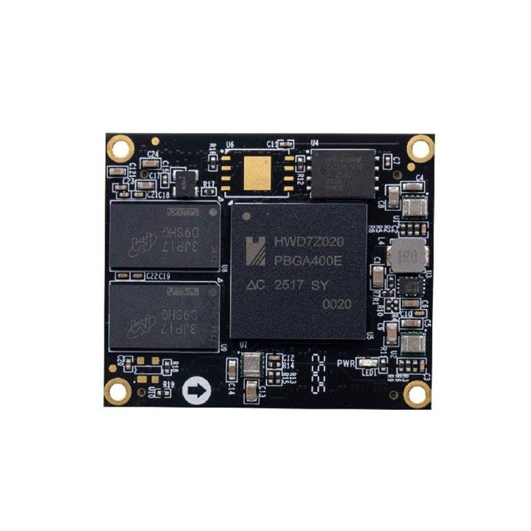
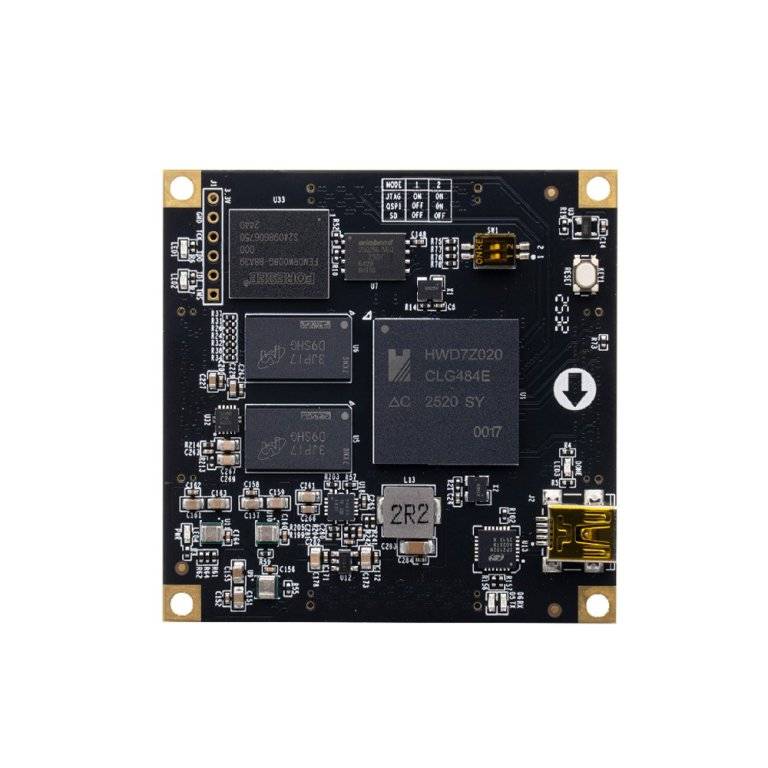
ZYNQ’s value is that one chip holds both a dual-core ARM Cortex-A9 (PS, running system software, networking and the file system) and programmable logic (PL, doing parallel acquisition, protocol acceleration and real-time IO). When an XC7Z020 design must go domestic, the goal is not a totally different architecture but a domestic drop-in compatible in instruction set, peripherals and the Vivado flow. PBC7Z020G carries HWD7Z020-1PBGA400 and PBC7Z021G carries HWD7Z020-1CLG484; both are domestic industrial-grade, dual-core A9@800MHz plus FPGA heterogeneous, natively Vivado-compatible with no extra patch, and rated -55~125°C ultra-wide temperature.
Before migrating, split the project into three layers and estimate each:
1. PS software: bare-metal programs, FreeRTOS tasks, Linux apps and drivers running on the A9.
2. PL logic: RTL, IP cores, constraints and pin mapping written in Vivado, running in the FPGA fabric.
3. Boot and BSP: boot image, QSPI/eMMC/SD boot config, device tree and board support package.
2. PS Software Migration: Highest BSP Reuse
1. Bare-Metal and FreeRTOS: The Project Barely Changes
Bare-metal and FreeRTOS projects call A9 peripheral interfaces (UART, GPIO, timers, interrupt controller) through the BSP. HWD7Z020’s PS register layout is compatible with XC7Z020, so SDK/BSP drivers are reusable and application-layer code needs no rewrite. Changes concentrate on regenerating the BSP under the domestic device library, recompiling, and checking interrupt numbers and clock config. The effort is measured in days, not months.
2. Linux: Local Adjustments to Device Tree, U-Boot and Kernel
For Linux designs the PS side changes more than bare-metal, but it is not a fresh start:
- Device tree (DTS): remap PS peripheral nodes and PL connection nodes from the XC7Z020 tree to the domestic board connectors; fill DDR3 capacity/width, eMMC/QSPI partitions, Ethernet/USB nodes for the new board.
- U-Boot and kernel: use an XC7Z020-compatible config to trim; adjust bootargs, console baud rate and rootfs mount; recompile and regression-test custom drivers on the domestic device.
- Application layer: user services, network programs and business algorithms are chip-independent and move over directly.
Estimate DDR3 bandwidth from the board config first: both PBC7Z020G/021G use DDR3 1GB, 32-bit bus, 1066Mbps; byte bandwidth = 4B × 1066MT/s ≈ 4.26 GB/s, enough for ordinary embedded control and light image transfer, so no platform swap is needed for bandwidth.
3. PL Logic Migration: Re-Plan Constraints After Resource Check
PL Resource Comparison (XC7Z020 Class vs HWD7Z020 / PBC7Z021G)
| Resource | XC7Z020 Class | PBC7Z021G (HWD7Z020-1CLG484) | Migration Call |
|---|---|---|---|
| Logic cells | ~85K | 85K | Same class, fits the design |
| LUT | ~53.2K | 53,200 | Same class |
| Flip-Flops | ~106K | 106,400 | Same class |
| DSP multipliers | 220 | 220 | Same class |
| Block RAM | 4.9 Mb | 4.9 Mb | Same class |
| Available PL IO | — | 198 (plus 48 LVDS pairs, 100 voltage-configurable IO) | Re-plan on new connectors |
The original RTL behavioral code, pure combinational/sequential logic and most IP cores (BRAM, FIFO, PLL/MMCM, AXI interconnect) synthesize directly under the compatible flow and need no rewrite.
Constraints, IP and Pin Re-Mapping
After the package moves from PBGA400 (020G, tiny 35×42mm) to 1CLG484 (021G, 60×60mm), physical pins and exposed IO differ, so the XDC constraint file must be re-assigned by the new board connectors; the power tree, DDR3 routing and clock crystals (021G carries a 33.33MHz PS crystal plus a 50MHz PL crystal) are also checked against the new board. If an IP uses a vendor-private hard block (certain transceivers, security modules), confirm whether the domestic device provides an equivalent IP; otherwise replace it with generic RTL.
4. Boot Chain and Landing Checklist
Boot Modes and Boot Image
PBC7Z021G reserves a 6-pin JTAG and supports JTAG / QSPI / SD card boot modes selected by a DIP switch; PBC7Z020G uses 2×120-pin Panasonic connectors and 5V supply. Land the migration by going through this checklist:
1. PS software: regenerate BSP, recompile and regression-test bare-metal/FreeRTOS; update device tree, U-Boot bootargs and kernel config for Linux.
2. PL logic: synthesize the original project, rewrite XDC constraints for the new package, check IP compatibility and timing closure.
3. Boot config: confirm boot mode (JTAG debug → QSPI/SD production), build boot.bin (FSBL, bitstream, device tree) and rootfs.
4. Wide temperature and reliability: domestic boards are -55~125°C (020G/021G); run thermal cycling and long-power-on tests for the target condition and confirm power margin.
Selection: Pick 020G / 021G / Pure-FPGA Expansion by Size and IO
- Ultra-small replacement (PBC7Z020G, ¥799): 35×42×5.5mm, 2×120-pin, for space-tight, medium-logic miniaturized embedded and replacement nodes.
- Fully-exposed production (PBC7Z021G, ¥999): 60×60mm, 4×80-pin, 198 PL IO and 48 LVDS pairs, PS/PL resources fully exposed, for engineering production and designs needing more external IO.
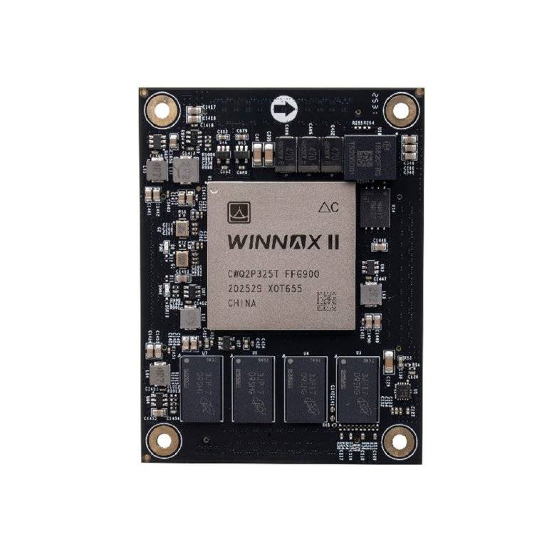
- Pure-FPGA large-resource expansion (PBC7K325G, ¥1,999): when the PL side needs high-speed transceivers or large logic (16 GTX lanes@12.5Gb/s, 2GB DDR3, 326K logic cells), a domestic Kintex-7 SoM takes over, complementing the ZYNQ scheme.
ZYNQ China replacement is not a rebuild: PS software and the application layer reuse the most; what you actually touch is re-planning PL constraints for the new package and updating the device tree and boot image. Split into PS, PL and boot layers to estimate each; within the compatible flow a project needs only local adjustment, with risk concentrated on IP compatibility and wide-temperature regression, so migration lands on schedule.