PCIe Bandwidth Planning: How Much Net Bandwidth Can You Really Get from Gen3 x4 to x16?
The PCIe bandwidth bill is far more complex than the number on the datasheet—raw bandwidth, coding overhead, protocol overhead, DMA efficiency, and the DDR bottleneck each eat into that “16 GB/s”. This article works through Gen3 x4/x8/x16, all the way to DDR and DMA matching, and gives a reusable method for estimating net bandwidth.
1. Three Layers of Bandwidth: Raw, Encoded, Net
When you see “PCIe Gen3 x16” on a spec sheet, your intuition says 16 GB/s. That number is actually the raw bit rate, not the bandwidth you can use in your system. Two layers of loss sit in between:
| Layer | Gen3 x16 calculation | Result | Meaning |
|---|---|---|---|
| ① Raw bit rate | 16 lanes × 8.0 GT/s | 128 Gb/s | Raw symbol rate on the link |
| ② Post-coding bandwidth | 128 × 128/130 (Gen3 uses 128b/130b) | ≈ 126 Gb/s ≈ 15.75 GB/s | Payload data rate after coding overhead |
| ③ Actual net bandwidth | 15.75 × transfer efficiency (80%–90%) | ≈ 12.6 – 14.2 GB/s | Real usable bandwidth after TLP headers, DMA descriptors, interrupts |
Gen3 runs 8.0 GT/s per lane with only 1.5% 128b/130b coding overhead—that is why Gen3 is far more efficient than Gen2 (which carries 20% 8b/10b overhead). Comparison across widths:
| PCIe width | Raw bit rate | Post-coding bandwidth | Typical net bandwidth (large-block DMA) |
|---|---|---|---|
| Gen3 x4 | 32 Gb/s | ≈ 3.94 GB/s | ≈ 3.2 – 3.5 GB/s |
| Gen3 x8 | 64 Gb/s | ≈ 7.88 GB/s | ≈ 6.3 – 7.1 GB/s |
| Gen3 x16 | 128 Gb/s | ≈ 15.75 GB/s | ≈ 12.6 – 14.2 GB/s |
| Gen2 x8 (reference) | 40 Gb/s | ≈ 4.0 GB/s (8b/10b) | ≈ 3.2 – 3.6 GB/s |
2. How Much Protocol Overhead: TLP, Payload, Read vs Write
Post-coding bandwidth is not net bandwidth. Every PCIe Transaction Layer Packet (TLP) carries a 12–20 byte header; the larger the payload, the smaller the header share, and the higher the efficiency.
Payload Size Directly Determines Efficiency
| Payload size | TLP header share | Transfer efficiency | Typical scenario |
|---|---|---|---|
| 4 KB (max) | ≈ 0.4% | ≈ 90%+ | Large-block continuous DMA acquisition, video streams |
| 512 B | ≈ 3% | ≈ 85–88% | General data return |
| 64 B | ≈ 25% | ≈ 55–65% | Register reads/writes, small-packet control |
Reads Are Slower Than Writes: The Hidden Cost of Completion
PCIe writes are fire-and-forget; the sender does not wait for acknowledgement. PCIe reads must wait for a Completion TLP to come back—a round trip that doubles latency and costs bandwidth. Measured:
- Large-block sequential writes: 88–92% of post-coding bandwidth
- Large-block sequential reads: typically only 80–85% (Completion queueing, overhead)
- Mixed read/write: direction switching causes link stalls, dropping efficiency another 5–10%
In engineering planning, use the conservative estimate “net bandwidth = post-coding × 80%”, not the ideal 90%+ figure, to leave headroom.
3. DDR Is the Real Ceiling
A fast PCIe link does not mean the system can run at full speed—data in and out of the FPGA must cross DDR, and DDR bandwidth is often the first wall you hit.
How to Calculate DDR Bandwidth
DDR bandwidth = data bus width × data rate / 8. For Duyuante’s common boards:
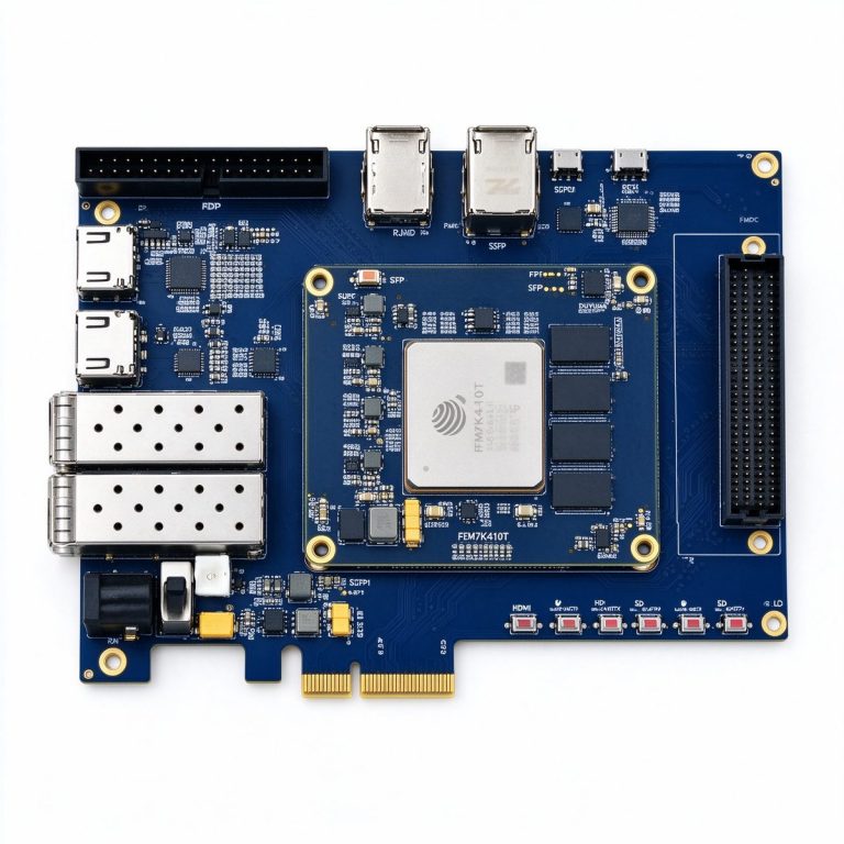
- DUK7410T: 4 GB DDR3, 64-bit bus, 1866 Mbps → 64 × 1866 / 8 ≈ 14.9 GB/s
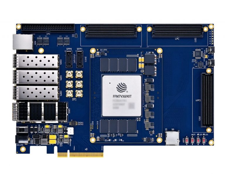
- DUF7690T: 4 GB DDR3, 64-bit, 1866 Mbps → ≈ 14.9 GB/s
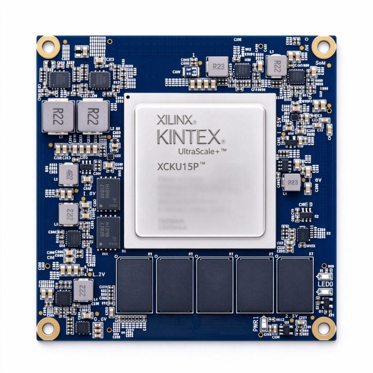
- DUKU15P: 8 GB DDR4 ECC, 64-bit bus (+8-bit ECC) → at 2400 MT/s ≈ 19.2 GB/s
Data Flow Is Bidirectional: Read + Write Double the Load
Consider a high-speed acquisition scenario: ADC data is processed by the FPGA and written back to the host over PCIe. That data path crosses DDR twice:
- FPGA receives data → DDR write (frame buffer)
- FPGA finishes processing → DDR read (fetches for transmission)
- Total DDR load = write bandwidth + read bandwidth
If PCIe x8 Gen3 net bandwidth is 7 GB/s, DDR must simultaneously write 7 GB/s and read 7 GB/s = 14 GB/s—approaching the DDR3 physical limit of 14.9 GB/s, leaving almost nothing for FPGA algorithm work. This is why x8 Gen3 paired with DDR3 is the “golden combo,” while x16 requires DDR4.
| Board | PCIe spec | Post-coding bandwidth | DDR config | DDR bandwidth | Match verdict |
|---|---|---|---|---|---|
| DUK7410T | Gen2 x8 | ≈ 4.0 GB/s | 4 GB DDR3 64-bit | ≈ 14.9 GB/s | PCIe is the bottleneck, DDR has headroom |
| DUF7690T | Gen3 x8 | ≈ 7.88 GB/s | 4 GB DDR3 64-bit | ≈ 14.9 GB/s | ~7.5 GB/s each way, just balanced |
| DUKU15P | Gen3 x16 | ≈ 15.75 GB/s | 8 GB DDR4 64-bit | ≈ 19.2 GB/s | DDR approaches its limit at full PCIe load |
4. Three-Step Estimation: How Much Bandwidth Does Your Project Need?
Methodology · 01: PCIe Bandwidth Estimation in Three Steps
Step 1: Calculate net demand. Sum the raw data rates of all data sources—the minimum volume that must be moved.
Step 2: Apply a redundancy factor. Multiply by 1.2–1.5 for overhead, bursts, and duplex.
Step 3: Back-calculate PCIe width. Choose a spec where post-coding bandwidth ≥ redundant demand, then verify DDR can keep up.
Validated against three common scenarios:
| Scenario | Raw data rate | Post-redundancy demand | Recommended PCIe | Why |
|---|---|---|---|---|
| High-speed acquisition (2ch × 250 MSPS × 14-bit) | ≈ 875 MB/s | ≈ 1.1 – 1.3 GB/s | Gen3 x4 (3.94 GB/s) | Ample headroom, DDR stress-free |
| 4K60 video capture & processing (10-bit 4:2:2) | ≈ 1.5 GB/s | ≈ 1.8 – 2.3 GB/s | Gen3 x8 (7.88 GB/s) | Room for multi-channel video or stitching |
| AI inference feature-map bulk return / 8K video | ≈ 10 – 12 GB/s | ≈ 12 – 18 GB/s | Gen3 x16 (15.75 GB/s) | Requires DDR4, or DDR hits the wall first |
A rule of thumb: when choosing PCIe width, back-calculate from net demand × 2, and leave a full factor of two headroom. You can upgrade bandwidth, but you cannot upgrade width without redesigning the board.
5. Choosing Among Duyuante’s Three PCIe Platforms
DUK7410T (¥9,999)—Cost-Sensitive Acquisition & Processing
Fudan Micro JFM7K410T, PCIe Gen2 x8 hard IP, ~4 GB/s post-coding. Pair with FMC HPC mezzanines for high-speed ADC acquisition, or HDMI 4K video processing—start here when PCIe bandwidth is not the bottleneck.
DUF7690T (¥24,999)—Mainstream Acquisition & Composite Processing
Fudan Micro JFM7VX690T, PCIe Gen3 x8 hard IP, ~7.88 GB/s post-coding. With 4 GB DDR3 at ~7.5 GB/s each way, it matches x8 full bandwidth. Mainstream platform for multi-channel acquisition, radar signal processing, and video stitching.
DUKU15P (¥15,999)—High-End Data Return & 100G Interconnect
AMD Kintex UltraScale+ XCKU15P, PCIe Gen3 x16 hard IP, 15.75 GB/s post-coding, paired with 8 GB DDR4 ECC. Integrates 56 high-speed transceivers (24× GTY 28G + 32× GTH 16G) and 4× 100G Ethernet hard IP—flagship choice for large-bandwidth PCIe return plus high-speed networking.
PCIe bandwidth is never just “interface speed”—it is the shortest board among “interface × memory × DMA”. Plan DDR headroom first, then talk about how fast PCIe can run.
>
— Duyuante R&D Team