The Real Cost of China FPGA Migration: A TCO Framework from Xilinx to FMSH/Pango
Domestic substitution is not as simple as “swapping one chip.” Many teams only compare unit price and logic resources during selection, only to discover once migration begins that toolchain, IP cores, PCB layouts, and engineer learning curves all need to be recalculated. This article gives you a TCO (Total Cost of Ownership) framework that itemizes every cost of migration, so you can decide whether it is worth doing.
1. Break Migration Cost into Four Blocks
Migrating a Xilinx project to China FPGA (FMSH JFM7 series, Pango Titan3 / Kosmo-2 series) is not a single-point expense but four parallel lines:
| Cost Item | Content | Typical Share |
|---|---|---|
| Toolchain migration | Vivado project flow, constraint files, IP Catalog, timing closure | 15%~25% |
| IP core rewrite | PCIe, DDR controller, SerDes PHY reconfiguration | 30%~40% |
| Hardware changes | BGA package differences, PCB layer redraw, power tree, clocking | 15%~25% |
| Labor & validation | Engineers learning new toolchain, board-level revalidation, timing iterations | 20%~30% |
Let’s break down each item.
2. Toolchain Migration: From Vivado to Domestic EDA
Xilinx projects use Vivado Design Suite. Migration targets map as follows:
| Original Platform | Domestic Target | Tool | Difficulty |
|---|---|---|---|
| Xilinx Vivado | FMSH JFM7 series | FMSH proprietary EDA | Medium — similar project structure, IP library remapping needed |
| Xilinx Vivado | Pango Titan3 / Kosmo-2 | Pango Design Suite (PDS) | Medium-Low — PDS UI close to Vivado, constraint syntax largely compatible |
What actually changes
- Constraint files: .xdc format is largely compatible, but pin numbering must be remapped (different BGA ball map).
- IP Catalog: Xilinx FIFO Generator, BRAM Controller, and PCIe IP cannot be reused directly; you must re-instantiate corresponding IP from the domestic vendor.
- Timing closure: Domestic FPGAs typically have slightly tighter timing margins at the same speed grade. A 100 MHz design with 20% margin on Xilinx may only have 5%~10% after migration, requiring critical-path optimization.
Cost estimate: A 3~5 person FPGA team needs about 2~4 weeks to learn the toolchain. At ~¥30k/person-month, this is roughly ¥20k~50k (one-time).
3. IP Core Rewrite: The Most Expensive Block
The toolchain is “relearning”; IP cores are “redoing.” This is the largest cost block in migration.
| IP Type | Xilinx Native | Domestic Equivalent | Rewrite Effort |
|---|---|---|---|
| DDR controller | MIG (DDR3/DDR4) | FMSH / Pango DDR PHY + controller | High: timing, calibration, training flow differ |
| PCIe hard block | Integrated Block for PCIe | FMSH PCIe Gen3 x8 / Pango PCIe Gen4 x8 | Medium: re-tune config, enumeration logic reusable |
| SerDes (GTX/HSST/MGT) | 7-series GTX / UltraScale GTH | FMSH GTX / Pango HSST | High: reference clock, pre-emphasis, equalization all re-tuned |
| FIFO / BRAM / DSP | Block RAM Generator / FIFO Generator | Domestic vendor equivalent IP | Low: regenerate, logic reusable |
Why is IP rewrite expensive? High-speed interface IP (DDR, PCIe, SerDes) is not just “changing a parameter” — it involves board-level signal integrity. The original PCB routing was tuned to Xilinx reference designs; after switching to a domestic PHY, eye diagrams must be remeasured, equalization parameters re-found, and link training re-run. This is often the most uncontrollable part of a migration project.
Cost estimate: A project with PCIe Gen3 x8 + DDR4 + multiple high-speed transceivers typically needs 1.5~3 months for IP rewrite and bring-up, with labor cost around ¥80k~150k.
4. Hardware Changes: Does the PCB Need Redrawing?
It depends on which domestic chip you target:
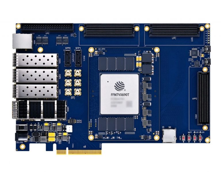
- FMSH JFM7 series (pin-compatible with Kintex-7 / Virtex-7): BGA pin definitions are highly compatible with Xilinx 7 series. The PCB can be a pin-to-pin swap — no layer redraw needed, only the chip part number and power net change. This is the lowest-cost migration path.
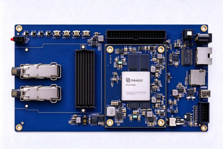
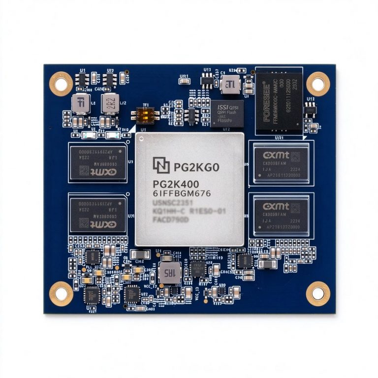
- Pango Titan3 / Kosmo-2 (new architecture): BGA packages are incompatible with Xilinx. The PCB must be redrawn from scratch — power tree, clock distribution, high-speed routing all follow the new chip’s reference design.
| Migration Path | PCB Change | Hardware Cost (one-time) |
|---|---|---|
| Xilinx Kintex-7 → FMSH JFM7K325T/K410T | Pin-to-pin, minor revision | ¥10k~30k (PCB fab + materials) |
| Xilinx Kintex-7 → Pango Titan3 | New PCB | ¥50k~100k (4~6 layer redraw + 2~3 fab rounds) |
| Xilinx ZYNQ → Pango Kosmo-2 SoPC | New PCB + ARM BSP port | ¥80k~150k (including software BSP) |
5. Labor TCO: Don’t Just Count the “Board Cost”
Many teams only compare chip unit prices during selection, ignoring labor. A realistic TCO for a migration project:
| Cost Item | Small (single card / prototype) | Medium (product-level board) | Large (multi-board / mass production) |
|---|---|---|---|
| Toolchain learning | 2~4 weeks / ¥20k~50k | 4~6 weeks / ¥50k~80k | 6~8 weeks / ¥80k~120k |
| IP core rewrite | 1 month / ¥50k~80k | 2~3 months / ¥100k~150k | 3~6 months / ¥200k~400k |
| PCB changes | ¥10k~30k | ¥50k~100k | ¥100k~200k |
| Board validation & iteration | 2~4 weeks / ¥20k~40k | 1~2 months / ¥50k~100k | 2~3 months / ¥150k~300k |
| Total TCO | ~¥100k~200k | ~¥250k~450k | ~¥500k~1,000k |
These numbers look large, but against two background factors:
- Chip unit price is genuinely lower: Xilinx Kintex-7 XC7K410T is ~¥3,000~4,000/unit; FMSH JFM7K410T is ~¥1,500~2,000/unit. The more volume, the more you save.
- Supply security is an intangible benefit: Xilinx chips have long import lead times and allocation uncertainty; domestic chips can be sourced locally in 2~4 weeks. This cost is hard to quantify but critical for production programs.
6. When Is Migration Worth It?
Not every project should migrate. We usually evaluate three conditions:
1. Long project lifecycle (>2 years): Migration cost is one-time; the longer the lifecycle and higher the volume, the more unit-price savings amortize the migration investment.
2. High supply certainty requirements: Military, industrial, and medical sectors where supply chain security is sensitive gain the most intangible benefit from migration.
3. Original design uses 7-series (Kintex-7 / Artix-7): 7-series has direct FMSH JFM7 compatible parts, with the shortest and lowest-cost migration path. UltraScale+ / Versal do not yet have mature domestic alternatives — do not force migration.
China FPGA migration is not a “cheap or expensive” question — it is whether a one-time investment can be amortized by volume and supply security. Calculate the TCO before deciding whether to move.
>
— Duyuan Engineering Team