The Last Wave of the 28nm Era: Why People Still Buy Kintex-7 in 2026 Instead of Jumping Straight to UltraScale+
It is 2026. AMD’s newest Versal AI Edge has been on sale for years, and UltraScale+ is already a process node from a decade ago. Yet a significant share of the inquiries Duyuan Electronics receives every week still explicitly specify Kintex-7 (XC7K325T, XC7K410T, XC7K160T). Not because these customers cannot afford UltraScale+, but because in many real products Kintex-7 is actually the more rational choice. This article walks through four typical scenarios.
1. First, the Generational Gap: What Actually Differs Between Kintex-7 and Kintex UltraScale+
Many engineers’ first instinct in FPGA selection is “buy new, not old.” But when you lay the datasheets side by side, the two are not simply “new vs. old” — they are two tiers, two process technologies, and two completely different cost structures.
| Parameter | Kintex-7 XC7K325T | Kintex US+ XCKU15P |
|---|---|---|
| Process node | 28nm HPL (2011) | 16nm FinFET (2016) |
| Logic cells (LC) | 326K | 1,143K (≈3.5×) |
| DSP slices | 840 | 1,968 |
| Block RAM | 16,020 Kb | 34.6 Mb + 36 Mb UltraRAM |
| High-speed transceivers | 8 × GTP @ 10.3 Gbps | 24 × GTY @ 28G + 32 × GTH @ 16G |
| PCIe | Gen2 ×8 | Gen3 ×16 hard core |
| Typical chip price (per 1K) | ≈ ¥300–500 | ≈ ¥6,000–8,000 |
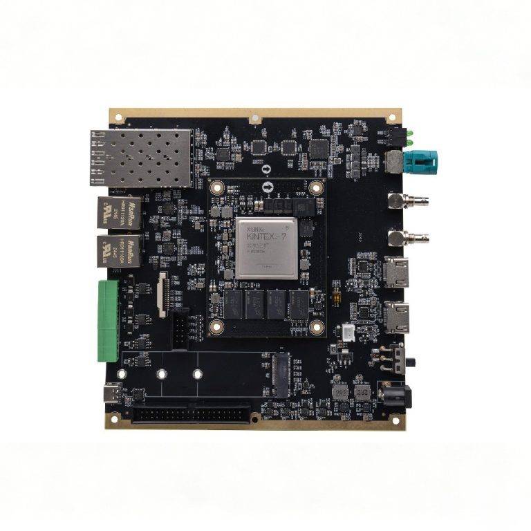
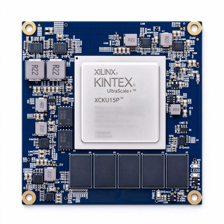
| Typical SOM/dev-board price | ¥8,999 (PB7K325) | ¥15,999 (DUKU15P) |
On paper, the XCKU15P wins across the board — 3.5× the logic, transceivers jumping from 10G to 28G, PCIe from Gen2 to Gen3. But if your product only needs 8 lanes of 6 Gbps serial I/O, does not need 100G optical ports, and Gen2 PCIe is enough, then all these “upgrades” are premiums you will never use.
2. Why People Still Buy Kintex-7 in 2026: Four Real Scenarios
Scenario 1: Cost-Sensitive High-Volume Industrial Products — Saving ¥3,000 Per Chip Adds Up to Millions a Year
Industrial cameras, motor drives, data acquisition cards, protocol converters — in these products the FPGA is usually only 5%–10% of the BOM, but the end price is locked at a few thousand yuan. For an industrial camera project shipping 10K units a year, switching the main FPGA from XC7K325T to XCKU15P raises the per-chip cost from ¥400 to ¥7,000 — adding ¥6,600,000 to the annual BOM. Meanwhile your camera only goes from 5MP to 12MP resolution, and GigE from 1G to 10G, still using 4 pairs of 6.25 Gbps GTP transceivers. Kintex-7 is more than enough.
The selection logic for this category of product is very direct: good enough, cheap, and reliably supplied. The 28G GTY, UltraRAM, and PCIe Gen3 of UltraScale+ are pure overhead for an industrial camera running GigE Vision.
Scenario 2: Long-Lifecycle Products — Medical, Industrial Instrumentation and High-Reliability Equipment Sold Over 10–15 Years
Medical ultrasound, industrial PLCs, railway control, and high-reliability radios — once these products pass certification (FDA / CE / CRCC / GJB), the platform must be supplied steadily for 10+ years. Kintex-7 has been in mass production since 2011 — 15 years now — and Xilinx’s committed supply horizon is far longer than for UltraScale+ (which entered mass production in 2016; following Xilinx’s usual 10–15 year lifecycle, it may enter the phase-down window in 2028–2031).
For medical device makers, the worst fear is not insufficient performance but the chip going end-of-life mid-production. Re-spinning the PCB and re-running medical certification starts at hundreds of thousands of USD. In this scenario Kintex-7 is the opposite of “newer but safer” — it is old enough that it is “not going to be discontinued casually.”
Scenario 3: Proven Existing Designs — Changing the Chip Means Redesigning the PCB and Re-Tuning Signal Integrity
Many customers have a Kintex-7 design running for five years, with I/O assignments, power tree, and PCB stack-up all finalized. Want to upgrade performance? Switching the BGA from FFG676 to FFBV1517 means:
- Package goes from 27×27mm to 45×45mm — PCB must be re-laid out
- Power changes from 1.0V/1.2V to a multi-phase 0.85V/0.9V/1.8V tree — the power design starts over
- 80 HP I/O pairs become 236, board layers go from 6 to 16, impedance recalculated
- Transceivers move from GTP @6.25G to GTH @16G, connectors from 1.27mm headers to 0.8mm high-speed board-to-board
This is not “swap a chip” — this is redesigning the board. If your existing Kintex-7 design is stable and volumes justify it, the most rational move is to keep doing small iterations on Kintex-7 (add a Flash, optimize the power) rather than forcing an UltraScale+ migration.
Scenario 4: Performance Headroom — Many Applications Never Use 16G/28G
The core selling points of Kintex UltraScale+ are the 28G GTY and 100G Ethernet hard cores. But look back at real mid/low-speed applications:
- Motor control, PLC, motion controllers: LVDS / RS485 / EtherCAT, up to 125 Mbps
- Industrial cameras, image acquisition: Camera Link, GigE Vision, up to 6.25 Gbps
- Protocol conversion, interface bridging: USB 2.0, CAN FD, SPI, UART — all low-speed
- Logic control, state machines, custom ASIC prototyping: only consume LUTs, not high-speed transceivers
In these cases, the 24 GTY lanes you paid ¥7,000 for sit idle — like buying a truck to go grocery shopping. Kintex-7’s 8 GTP lanes at 10.3 Gbps far exceed the requirement, and the money saved is better spent on mechanics, sensors, or algorithms.
3. When You Should Jump Straight to UltraScale+
Of course, Kintex-7 is not universal. The following categories of application must go directly to UltraScale+ without hesitation:
- 25G/40G/100G optical ports: 100G Ethernet, OTN, CPRI/eCPRI fronthaul, 150G Interlaken — Kintex-7 tops out at 10.3 Gbps GTP, physically unsupported
- PCIe Gen3 x8/x16: data acquisition cards, smart NICs, FPGA accelerator cards back-hauling to the host
- Logic capacity > 400K LC: cannot fit in a single chip; even the largest Kintex-7, the XC7K480T, only has 496K LC
- 8K video processing, radar pulse compression, high-frequency trading FPGA acceleration: needs UltraRAM (36Mb-class on-chip SRAM) and 2000+ DSPs
- Products requiring -2/-3 speed grades at 0.9V low power: Kintex-7 has no FinFET; at the same performance it draws 40%–60% more power
4. Duyuan’s Portfolio: Both Ends Covered
Duyuan Electronics deliberately built a “two-end portfolio” so that customers with different budgets and product lifecycles can pick a board that fits directly, without compromising on a single chip.
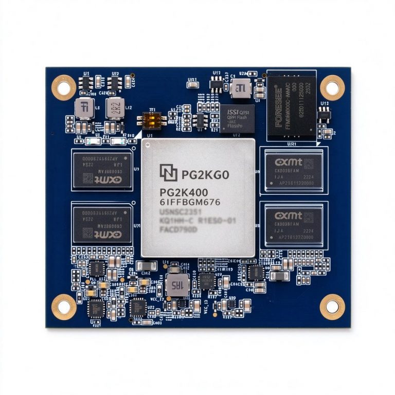
For high-volume, cost-sensitive, long-lifecycle products, use the PB7K325 (Kintex-7 XC7K325T development board, ¥8,999); for high-end products that need 100G, PCIe Gen3, and large logic capacity, use the DUKU15P (Kintex UltraScale+ XCKU15P SOM, ¥15,999). In between, we also offer domestic alternatives based on PangoMicro Titan3 / Kosmo-2.
“Buy new, not old” is consumer-electronics logic. In industrial FPGA selection, the logic is “good enough, cheap, and reliably supplied.” The 28nm Kintex-7 is still the optimal answer for many products in 2026 — provided you have truly thought through where your application’s boundary lies.
References
- AMD/Xilinx, Kintex-7 vs Kintex UltraScale+ product comparison: https://www.amd.com/en/products/adaptive-socs-and-fpgas/fpga/kintex-ultrascale-plus.html
- AMD/Xilinx, 7 series FPGA product selection guide: https://www.amd.com/en/products/adaptive-socs-and-fpgas/fpga/kintex-7.html
- Duyuan Electronics product pages, PB7K325 Kintex-7 board and DUKU15P XCKU15P SOM: https://www.profpga.net/product-category/product/amd-xilinx-fpga-core-board/