Migrating to the China FPGA Toolchain PDS: The Real Steps from Vivado to Pango/FudanMicro
Many people assume domestic migration is mostly about swapping the chip, but the first hurdle is actually the toolchain. Moving from Vivado to Pango’s PDS, or to FudanMicro’s EDA, changes how you open a project, write constraints, instantiate IP and close timing. This article walks through the migration step by step, what changes in each step, the pitfalls we hit, and the typical effort involved.
First, understand: Pango and FudanMicro are not the same migration path
Going from Vivado to a domestic toolchain, many assume “it’s just another EDA.” In reality Pango and FudanMicro differ a lot, so first work out which line you face:
| Target chip | Toolchain | How the project opens | Migration difficulty |
|---|---|---|---|
| Pango Titan3 / Kosmo-2 | Pango Design Suite (PDS) | Project structure, IP library and constraint syntax all differ from Vivado | Medium, flow is Vivado-like but the project must be rebuilt |
| FudanMicro JFM7 series | FudanMicro EDA | 7-series compatible devices, similar project structure | Medium-low, IP library needs re-mapping |
Pango goes the “new architecture + its own PDS” route, so a Vivado project basically has to be rebuilt; FudanMicro goes the “7-series compatible + similar flow” route, so more of the project can be reused. The steps below are generic and apply to both.
Step one: split the Vivado project, don’t move it whole
The Vivado `.xpr` project file does not open in a domestic toolchain. The right approach is to split the project into parts you can “reassemble”:
1. RTL source: `.v` / `.vhd` files are plain text and reuse as-is, no changes needed (as long as they do not depend on Xilinx private primitives).
2. Constraints: most `.xdc` syntax is readable, but pin assignment and clock definitions must be rewritten for the new device.
3. IP cores: Xilinx FIFO/BRAM/PCIe/DDR IP cannot be used directly; instantiate the corresponding IP from the domestic vendor instead.
4. Simulation and test: the `tb` bench is reusable, but the IP library paths used for simulation need to change.
The effort involved
A 3–5 person FPGA team typically spends 3–5 working days splitting the project and rebuilding the skeleton in the domestic toolchain. The real cost is not here, but in constraints and IP below.
Step two: the constraint file is the first trip point
`.xdc` syntax is very close to Vivado, but the details differ and cause the most pitfalls:
- Pin assignment: the BGA Ball Map differs, so `set_property PACKAGE_PIN` must be re-done against the new device. Pango uses the `PACE` pin tool in PDS; FudanMicro uses a similar flow.
- Clock constraints: `create_clock` / `create_generated_clock` syntax is compatible, but clock-source resource names (crystal, MMCM/PLL) must change.
- IO standards: LVDS, LVCMOS and bank voltage settings are re-done against the new device datasheet.
Practical tip: do a first pin assignment in PDS with `PACE`, or in the FudanMicro pin tool, then export the constraints. That is far more reliable than hand-writing `.xdc` and saves several rounds of fixes.
Step three: the IP re-instantiation checklist (cost core)
This is the largest part of the migration cost. The effort differs greatly by IP type:
| IP type | Vivado native | Domestic replacement | Effort |
|---|---|---|---|
| DDR controller | MIG (DDR3/DDR4) | Domestic DDR PHY + controller | High: timing, calibration, training flow differ |
| PCIe hard core | Integrated Block for PCIe | Domestic PCIe PHY + enumeration | Medium: re-tune config parameters, logic reusable |
| High-speed transceivers | GTX / GTH / HSST | Domestic transceiver PHY | High: ref clock, pre-emphasis, equalization re-tuned |
| FIFO / BRAM / DSP | Generator IP | Domestic vendor IP | Low: regenerate, logic reusable |
| PLL / MMCM | Clocking Wizard | Domestic clock IP | Low: re-enter parameters |
Any high-speed interface IP (DDR, PCIe, SerDes) is not “change a parameter and done” — it involves board-level signal integrity. The PCB was routed to Xilinx reference design; after switching to a domestic PHY, the eye diagram must be re-measured, equalization re-tuned and link training re-run. This is usually the least controllable part of a migration, so budget at least 2–4 weeks.
Step four: timing closure and iteration
Domestic FPGAs usually leave tighter timing margin than Xilinx at the same tier; a 100 MHz design with 20% margin may end up with only 5–10% after migrating. What to do:
1. Re-synthesize and place-and-route in the domestic toolchain, and read the timing report (PDS `Report Timing` / the FudanMicro equivalent).
2. Locate critical paths and optimize the RTL or add pipeline stages.
3. Iterate synthesis until timing closes.
This usually takes 1–2 weeks, depending on design complexity and original timing margin.
Landing checklist and typical schedule
One “Vivado → domestic toolchain” migration, chaining the four steps above, typically looks like:
| Step | Content | Typical time |
|---|---|---|
| Split project | Reuse RTL, rebuild skeleton | 3–5 days |
| Rewrite constraints | Re-do pins/clocks/IO standards | 3–5 days |
| Re-instantiate IP | DDR/PCIe/transceivers dominate | 2–4 weeks |
| Timing closure | Synthesis + routing + iterate | 1–2 weeks |
| Board verification | Bring-up, eye diagram, link regression | 2–4 weeks |
A medium-complexity project totals about 1–2 months, with cost concentrated in IP re-instantiation and timing closure.
Board selection advice: how to build the domestic board set
When picking a board for a migration, first confirm which chip line the target is on, then pick the matching board:
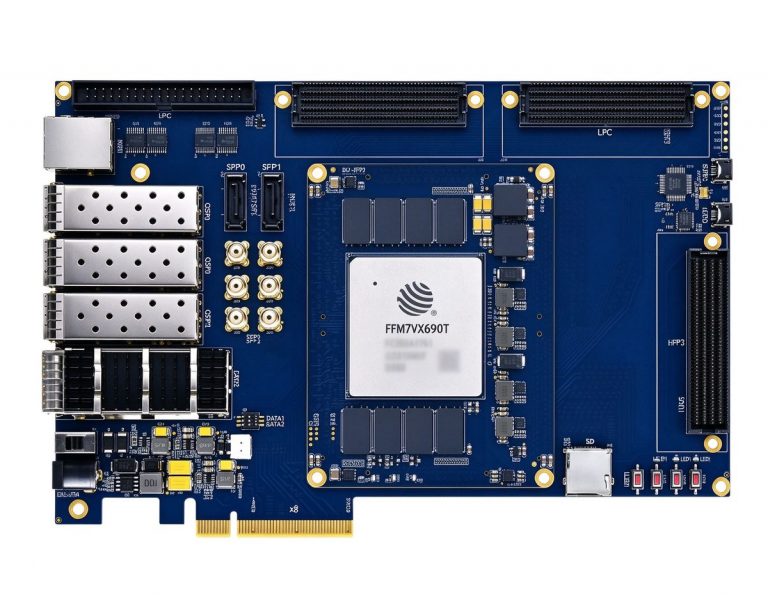
- FudanMicro JFM7VX690T (DUF7690T): Virtex-7-class resources, 7-series pin-compatible packaging, for pin-to-pin migration from Xilinx 7-series, industrial temperature.
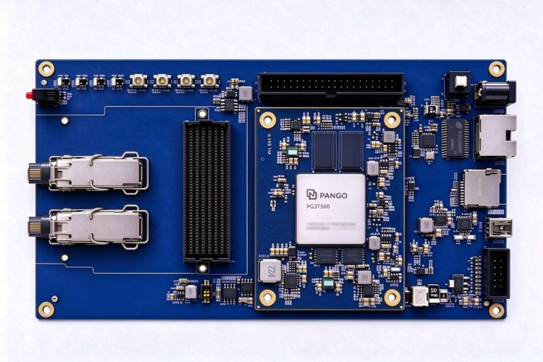
- Pango Titan3 (PG3T500): new-architecture high-end platform, for designs that need large resources and run the PDS flow.
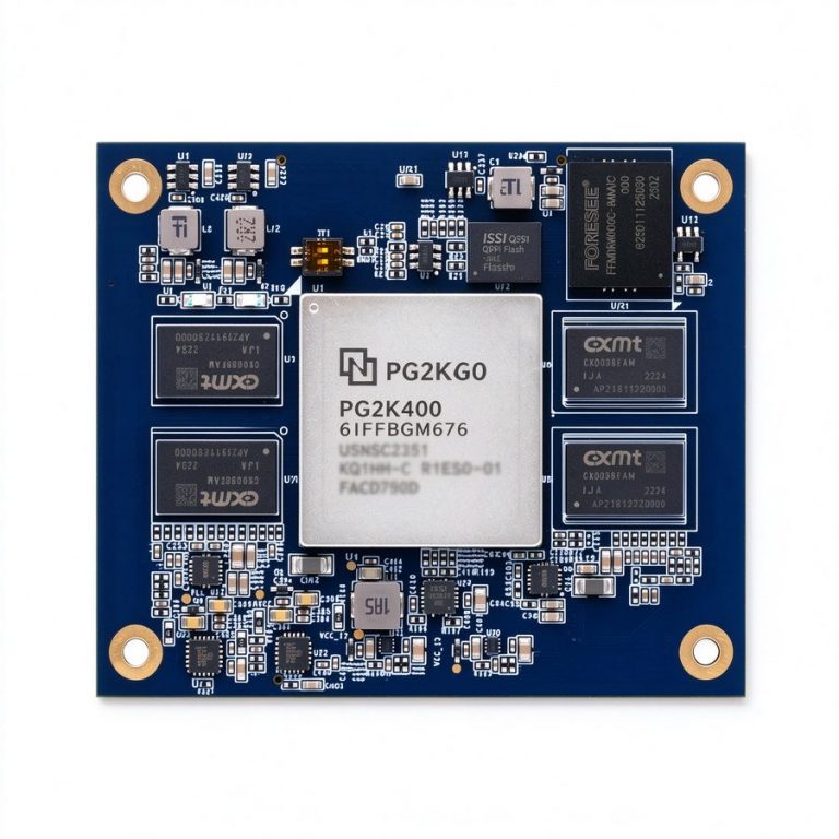
- Pango Kosmo-2 (PG2K400): ARM + FPGA heterogeneous, for ZYNQ/MPSoC-style designs moving to a domestic SoC.
The real barrier in a domestic toolchain migration is not whether the RTL can move, but that constraints, IP and timing all have to be re-done. Split the project first, rewrite constraints, focus effort on IP and timing closure, and plan the schedule and budget around “1–2 months, IP is the big item” — then the migration lands on plan instead of derailing halfway.
Further reading
- [The real cost of domestic migration: a TCO framework](/article/china-fpga-migration-tco-cost-framework/)
- [Domestic ZYNQ replacement in practice: from XC7Z020 to PBC7Z020G/021G](/article/zynq-china-replacement-pbc7z020-practical/)
- [How to pick an FPGA: a decision matrix of resources, transceivers and price](/article/fpga-selection-decision-matrix/)