
 China FPGA
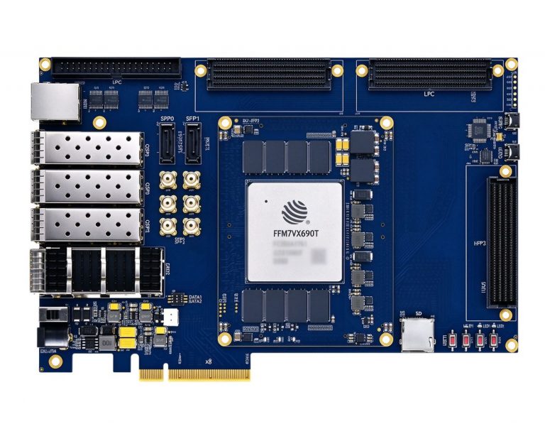
Fudan Micro JFM7VX690T China Virtex-7 FPGA Development Board DUF7690T
$3,846Tax not included View details →
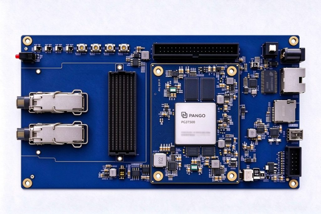
The DUPG3T500 is built on the Pango Titan3 series PG3T500-6IFFBG676 China FPGA, integrating 242,176 LUT6 logic cells, 529,760 equivalent logic cells, ~12,288 DSP resources, on-chip PCIe Gen4 x8 hard block and 16 high-speed MGT transceivers. It follows a SoM + carrier board architecture and delivers five key upgrades over generic platforms: on-board 2×SFP+ cages land high-speed links directly — no FMC+ card needed for 1G/10G fiber; dual Ethernet (GbE + 2.5G) utilizes both on-chip EMACs, one for management/upstream and one for data acquisition or time sync; DDR4 upgraded from 2GB to 4GB with ECC, targeting video/image processing, radar data buffering and long-running industrial scenarios; 16GB eMMC replaces the pluggable Micro SD as the boot device, offering shock and dust resistance for industrial deployment; and the fixed 200MHz oscillator is replaced by a programmable clock (Si5341-class, China-compatible) supporting 100/156.25/200MHz outputs and SFP recovered clock, covering JESD204, multi-board sync and PRBS eye-diagram testing. The BOM increase for all five upgrades totals approximately $30–50 per unit; the reference price of $923 is significantly lower than the typical ~$1,200+ landing cost of a generic board plus FMC+ SFP card. The SoM can be shipped standalone for customer prototype-to-product migration.
Interface, cooling, structure and batch supply can be customized per project · we respond within 1 business day after submission.
The DUPG3T500 is built on the Pango Titan3 series PG3T500-6IFFBG676 China FPGA, integrating 242,176 LUT6 logic cells, 529,760 equivalent logic cells, ~12,288 DSP resources, on-chip PCIe Gen4 x8 hard block and 16 high-speed MGT transceivers. It follows a SoM + carrier board architecture and delivers five key upgrades over generic platforms: on-board 2×SFP+ cages land high-speed links directly — no FMC+ card needed for 1G/10G fiber; dual Ethernet (GbE + 2.5G) utilizes both on-chip EMACs, one for management/upstream and one for data acquisition or time sync; DDR4 upgraded from 2GB to 4GB with ECC, targeting video/image processing, radar data buffering and long-running industrial scenarios; 16GB eMMC replaces the pluggable Micro SD as the boot device, offering shock and dust resistance for industrial deployment; and the fixed 200MHz oscillator is replaced by a programmable clock (Si5341-class, China-compatible) supporting 100/156.25/200MHz outputs and SFP recovered clock, covering JESD204, multi-board sync and PRBS eye-diagram testing. The BOM increase for all five upgrades totals approximately $30–50 per unit; the reference price of $923 is significantly lower than the typical ~$1,200+ landing cost of a generic board plus FMC+ SFP card. The SoM can be shipped standalone for customer prototype-to-product migration.
| Parameter | Specification |
|---|---|
| Board Model | DUPG3T500 V1.0 |
| FPGA Chip | Pango Titan3 PG3T500-6IFFBG676 |
| Chip Grade | Industrial; temperature range -40°C ~ 85°C |
| LUT6 Logic Cells | 242,176 |
| Equivalent Logic Cells (LC) | 529,760 |
| Flip-Flops | 484,352 |
| Distributed RAM | 6.3 Mb |
| On-chip Block RAM | DRM 616×36Kb + HRM 68×288Kb + APM 1804 |
| Clock Resources | GPLL ×4 / PPLL ×8 / FPLL ×7 |
| High-speed Transceivers (MGT) | 16 channels |
| PCI Express | On-chip hard block PCIe Gen4 x8 (gold-finger version reserved) |
| Ethernet MAC | 2× EMAC |
| User I/O | HPIO 98 / HDIO 54 |
| On-board Memory | 4GB DDR4 + ECC: 2× 2GB data dies (64-bit) + ECC parity |
| Boot Storage | 16GB eMMC on-board (Micro SD slot retained for expansion) |
| Configuration Storage | 2× 32MB QSPI Flash (FPGA configuration + user data) |
| Clock Source | Programmable clock (Si5341-class, China-compatible; 100/156.25/200MHz multi-output) |
| Fiber Interface | 2× SFP+ cages on-board (MGT direct, 1/10G optical modules) |
| Ethernet | Dual: 1× GbE RGMII + 1× 2.5G RGMII PHY |
| FMC+ Expansion | 1× FMC+: 34 LA differential pairs + 2 clock pairs + remaining MGT |
| Debug Interface | USB-to-UART · 10-pin JTAG · 40-pin 2.54mm expansion header |
| User Interaction | 7× LED + 4× push buttons + 1× reset |
| Power | +12V input; on-board multi-rail power tree (0.85V/1.2V/1.8V/3.3V) |
| PCB | SoM 80×60mm · Carrier 190×106mm · 2× 240-pin board-to-board connectors |
| Cooling | Active: aluminum heat sink + fan (standard); passive heat sink optional |
Industrial sites impose strict requirements on control equipment: wide temperature range, interference immunity and deterministic latency. FPGA handles real-time control, protocol parsing and high-speed I/O acquisition with reconfigurable parallel logic, providing a highly reliable hardware foundation for PLC expansion, motion control and industrial communication buses. Duyuan industrial-grade boards support a -40~85°C wide temperature range and long-term stable supply, helping devices move from prototype verification to mass production.
5G/6G base stations and high-speed network equipment impose strict requirements on protocol processing, data forwarding and deterministic latency. With high-speed transceivers, reconfigurable protocol stacks and parallel pipelines, FPGA powers 100G optical communication, protocol processing and network security acceleration, providing a high-throughput, low-latency hardware platform from R&D to mass production.
4K/8K video, machine vision and industrial cameras impose strict requirements on end-to-end latency and interface coverage. With hardware-direct video paths and parallel pipelines, FPGA delivers microsecond-level deterministic processing in video encoding/decoding, image pre-processing, multi-protocol interfaces and low-latency transport, supporting deep customization of video services and vision algorithms.
China FPGA
 China FPGA
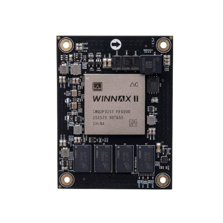
China FPGA industrial-grade SoM · CWQ2P325T · 326K logic · 16 GTX · 2GB DDR3
 China FPGA
We respond within 1 business day after submission, supporting selection consulting, parameter customization and batch supply.
Contact · +86 18621324348