
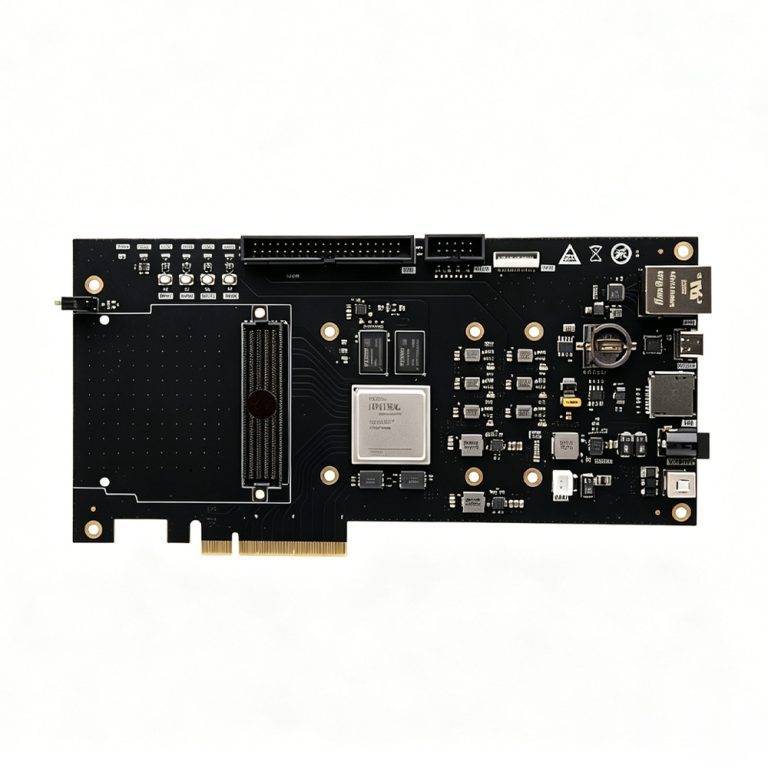
 FPGA Development Boards
AMD Xilinx Kintex UltraScale+ XCKU5P Development Board – FPGA Board
Kintex UltraScale+ high-performance development board · PCIe Gen3 x8 · GTY 28G transceivers · 475K logic
$384.46Tax not included View details →
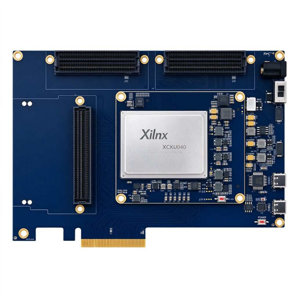
The DUKU040 is built around the Xilinx Kintex UltraScale XCKU040-2FFVA1156I industrial-grade FPGA, integrating 530K logic cells, 242,400 LUTs, 484,800 flip-flops, 1920 DSP slices, and 21.1Mb Block RAM, with 20 pairs of GTH transceivers (up to 16.3 Gbps per lane). The 83.8×64.8mm core board brings out all IOs through 168P board-to-board connectors, integrating 8GB DDR4 (64-bit), 512Mb QSPI, and 16GB eMMC. The 195×105mm carrier exposes 1×FMC HPC (8 GTH pairs, 144 IOs) + 2×FMC LPC (1 GTH pair, 72 IOs each), PCIe 3.0 x8, 2×SFP+ cages, dual Gigabit Ethernet, HDMI 1.4 output, with 200MHz + 125MHz differential clocks. Fully compatible with the Vivado design suite, it provides rich reference designs for LED, UART, DDR4, PCIe, and Ethernet, ready for high-speed data acquisition, software-defined radio, radar signal processing, machine vision, and high-speed communication prototyping.
Interface, cooling, structure and batch supply can be customized per project · we respond within 1 business day after submission.
The DUKU040 is built around the Xilinx Kintex UltraScale XCKU040-2FFVA1156I industrial-grade FPGA, integrating 530K logic cells, 242,400 LUTs, 484,800 flip-flops, 1920 DSP slices, and 21.1Mb Block RAM, with 20 pairs of GTH transceivers (up to 16.3 Gbps per lane). The 83.8×64.8mm core board brings out all IOs through 168P board-to-board connectors, integrating 8GB DDR4 (64-bit), 512Mb QSPI, and 16GB eMMC. The 195×105mm carrier exposes 1×FMC HPC (8 GTH pairs, 144 IOs) + 2×FMC LPC (1 GTH pair, 72 IOs each), PCIe 3.0 x8, 2×SFP+ cages, dual Gigabit Ethernet, HDMI 1.4 output, with 200MHz + 125MHz differential clocks. Fully compatible with the Vivado design suite, it provides rich reference designs for LED, UART, DDR4, PCIe, and Ethernet, ready for high-speed data acquisition, software-defined radio, radar signal processing, machine vision, and high-speed communication prototyping.
| Parameter | Specification |
|---|---|
| Product Model | DUKU040 V1.0 |
| FPGA Chip | Xilinx Kintex UltraScale XCKU040-2FFVA1156I |
| Speed Grade / Temp | -2 speed grade · Industrial -40°C ~ 85°C |
| Logic Cells / LUTs | 530K Logic Cells · 242,400 LUTs |
| FF / DSP / BRAM | 484,800 Flip-Flops · 1920 DSP Slices · 21.1 Mb Block RAM |
| GTH Transceivers | 20 pairs TX/RX, up to 16.3 Gbps per lane |
| PCI Express | 1× PCIe Gen3 x8 hard block (8.0 GT/s) |
| User I/O | 296 single-ended / 148 differential pairs (HR 1.8/2.5/3.3V, HP 1.2/1.8V selectable) |
| On-board Memory | 8GB DDR4 (64-bit, up to 2400 Mbps) |
| On-board Storage | 16GB eMMC · 512Mb QSPI Flash (2×256Mb) |
| Boot Modes | JTAG · QSPI · eMMC (DIP switch selectable) |
| On-board Clocks | 1×200MHz diff oscillator (FPGA) + 1×125MHz diff oscillator (GTH ref clock) |
| FMC Interfaces | 1 × FMC HPC (8 GTH, 144 IOs) + 2 × FMC LPC (1 GTH, 72 IOs each) |
| Optical Interfaces | 2 × SFP+ cages |
| Other Interfaces | 2 × Gigabit Ethernet · HDMI 1.4 output · UART · USB-JTAG · 4 user LEDs · 4 push buttons |
| Core Board Size | 83.8 × 64.8 mm · 168P board-to-board connector |
| Carrier Size | 195 × 105 mm · ENIG finish |
| Power Supply | +12V / 3A DC input |
5G/6G base stations and high-speed network equipment impose strict requirements on protocol processing, data forwarding and deterministic latency. With high-speed transceivers, reconfigurable protocol stacks and parallel pipelines, FPGA powers 100G optical communication, protocol processing and network security acceleration, providing a high-throughput, low-latency hardware platform from R&D to mass production.
From university labs to enterprise pre-research, rapidly verifying algorithms and hardware architectures is the critical first step to project success. Duyuan FPGA development boards and SoMs provide rich high-speed interfaces, complete reference designs and end-to-end technical support for ASIC prototype verification, high-speed data acquisition, instrument development and academic research — helping teams turn ideas into working hardware systems quickly.
4K/8K video, machine vision and industrial cameras impose strict requirements on end-to-end latency and interface coverage. With hardware-direct video paths and parallel pipelines, FPGA delivers microsecond-level deterministic processing in video encoding/decoding, image pre-processing, multi-protocol interfaces and low-latency transport, supporting deep customization of video services and vision algorithms.
Phased-array and imaging radar impose strict requirements on signal processing platforms: multi-channel parallel acquisition, high-throughput dataflow and deterministic low latency. With its reconfigurable parallel architecture, FPGA serves as the core carrier of radar signal processing, delivering multi-channel parallel, high-throughput, deterministic low-latency compute in beamforming, pulse compression and target detection, while supporting algorithm reconfiguration and platform evolution.
FPGA Development Boards
Kintex UltraScale+ high-performance development board · PCIe Gen3 x8 · GTY 28G transceivers · 475K logic
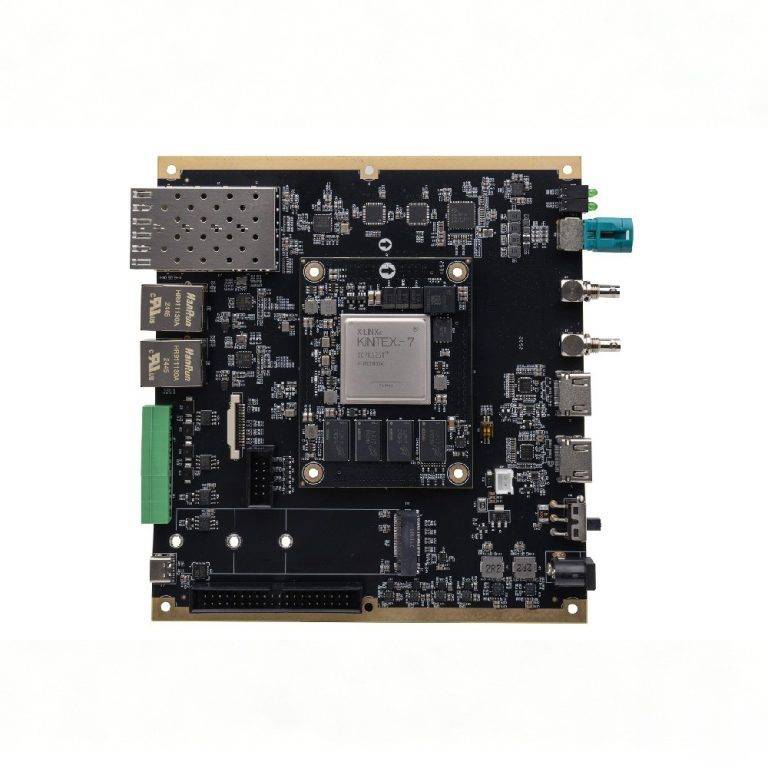 FPGA Development Boards
Kintex-7 high-performance video development board · 12G-SDI/GMSL2/10G optical · 4K/8K ultra-low-latency codec
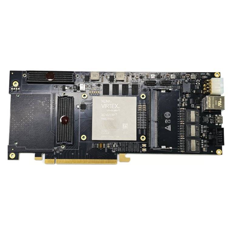 FPGA Development Boards
XCVU13P flagship PCIe development board · 3780K logic · dual FMC · OCULINK · 4GB DDR4
We respond within 1 business day after submission, supporting selection consulting, parameter customization and batch supply.
Contact · +86 18621324348