
Key Features
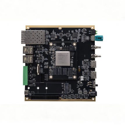
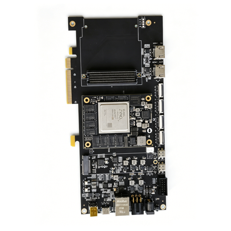
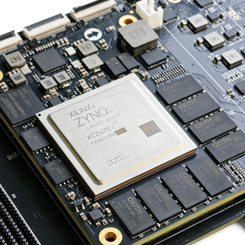
1. Main chip: Xilinx Zynq UltraScale+ EG ZU19EG with PS (Processing System) + PL (Programmable Logic) architecture, integrating a quad-core ARM Cortex-A53 and FPGA logic on a single chip.
2. PS memory: 5x DDR4 SDRAM chips totaling 10GB with ECC for reliable data operation.
3. PS storage: 32GB eMMC plus 2x 512Mb QSPI FLASH for boot and large-capacity data storage.
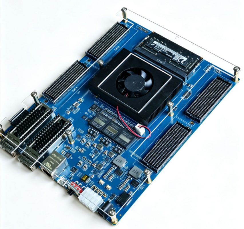
4. PL expansion: 260-pin DDR4 SODIMM socket on the PL side for external DDR4 SODIMM modules (sold separately).
Specifications
| Category | Details |
|---|---|
| Main Chip | Xilinx XCZU19EG-2FFVC1760I (industrial grade, -2 speed grade)
• PS:4×Cortex‑A53@1.3GHz + 2×Cortex‑R5F@533MHz PL: 1143K logic cells, 523K LUTs, 1045K flip-flops, 34.6Mb Block RAM, 1968 DSP slices, 44x GTH transceivers up to 16.3Gb/s |
| PS Memory | 5x Micron MT40A1G16KD-062E DDR4, total10GB with ECC; up to 2400 Mbps (1200 MHz), 72-bit bus |
| PL Memory Expansion | 260-pin DDR4 SODIMM socket (modulesold separately, connected to PL BANK69/70/71, 72-bit bus) |
| Non-Volatile Storage | 1. eMMC: Micron MTFC32GAPALBH-IT,32GB, 8-bit bus, e-MMC V5.0
2. QSPI FLASH: 2x Micron MT25QU512ABB1EW9-0SIT, 512Mb each (1Gb total), for U-Boot, bitstream and system images |
| Clock Sources | 1. PS reference clock: 33.333MHz
2. PL differential system clock: 200MHz 3. RTC: 32.768kHz crystal 4. Transceiver clock: Si5332BD-GM2 programmable clock for QSFP28, PCIe, M.2 and DP |
| Power | Board input:+12V DC;On-board DCDC/LDO regulators (MAX20796GFB, TPS6508640) providing multiple voltage rails for PS, PL, MGT transceivers and peripherals; RTC battery holder J22 for power-off timekeeping |
| Onboard Auxiliary Devices | EEPROM: 24LC04, 4Kbit I2C
Temperature sensor: LM75, I2C, 0.5°C accuracy ・LEDs:PowerLED: Power, DONE, PS user LED, PL user LED ・Buttons:1 side-mounted reset; 2 user buttons (PS/PL) ・4 DIP switch SW1: boot mode (JTAG, QSPI, eMMC, SD card) ・Cooling: heatsink + PWM-controlled fan |
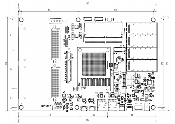
| Physical Dimensions | 250mm × 170mm |
1. High-speed Interfaces
| Interfaces | Specifications |
|---|---|
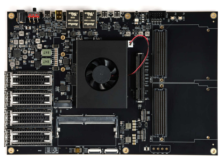
| QSFP28 Fiber Interfaces | 4 independent channels; 25Gbps per channel, 100Gbps total; OM4 multimode fiber up to 100m; connected to GTY transceivers BANK128‑131,Reference clock 156.25MHz; supports external QSFP28 optical modules (module sold separately) |
| PCIe x8 PCIe Edge Connector | PCIe3.0,8GBaud single channel; supports x8/x4/x2/x1 PCIe cards; MGT BANK226/227, 100MHz reference clock |
| M.2 M‑Key Interfaces | PCIe x1,PCIe-only M.2 SSD (no SATA), 6Gbps; connected to PS MGT BANK505 LANE1 |
| mini‑DP Display Output | DP1.2a;最高4K@30Hz /1080P@60Hz;Supports RGB, YCbCr formats; driven by PS MGT BANK505 LANE2/3 |
2. Network, USB, Serial
| Interfaces | Specifications |
|---|---|
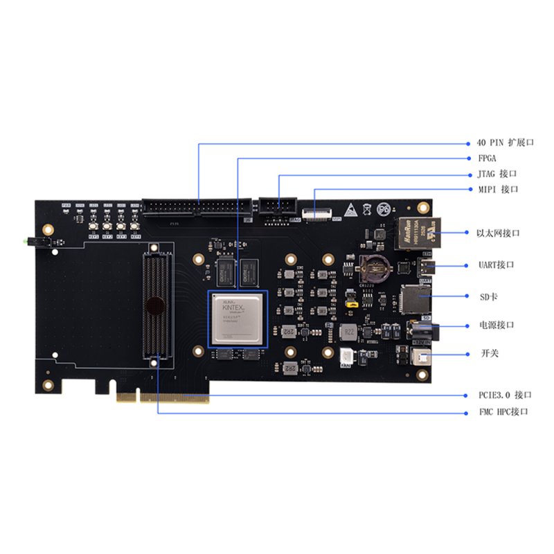
| Gigabit Ethernet RJ45 | 2 channels;PS、PL Each 1 channel; PHY KSZ9031RNX; 10/100/1000Mbps auto-negotiation, RGMII |
| USB3.0 Type‑A | 4 HOST mode, 5Gbps; external USB‑PHY USB3320C chip; supports mouse, keyboard, USB drive |
| USB‑UART(Type‑C) | 2 channels;PS、PL Each 1 channel; CP2102GM bridge; for PC debug serial, MINI‑USB Physical interface (manual says TYPE‑C,refer to actual hardware) |
3. Mezzanine Interfaces
| Interfaces | Specifications |
|---|---|
| Dual FMC‑HPC Expansion Ports(FMC1+FMC2) | FMC1:36 differential IO pairs + 8 GTH transceivers; IO voltage 1.8V/1.2V via jumper;
FMC2:60 differential IO pairs + 8 GTH transceivers; IO voltage 1.8V/1.2V via jumper; Supports third-party FMC modules: high-speed AD/DA, HDMI in/out, binocular cameras |
4. Multimedia & Storage
| Interfaces | Specifications |
|---|---|
| MIPI Camera Interface | 2‑lane MIPI CSI‑2,15PIN FPC connector; BANK68 differential IO; supports MIPI camera modules like OV5640 |
| Micro‑SD 卡槽 | TF card, TXS02612 level shifter; for BOOT, Linux image and file system; PS BANK501 MIO |
5. Debug & Auxiliary
| Interfaces | Specifications |
|---|---|
| JTAG Debug Port | 10Pin 2.54mm Header;with ESD protection; for FPGA/PS programming, debugging and FLASH burning; compatible with Xilinx programmers |
| RTC Battery Holder J22 | 2Pin 1.27mm pitch; external coin cell for RTC timekeeping, 32.768KHz crystal |
| Fan Connector J62 | 12V fan power, PL IO PWM speed control; fan + heatsink pre-installed |

Applications
1、High-speed Communications & Data Processing
- High-speed Fiber Communication Development:On-board 4x QSFP28 (25Gbps per channel, 100Gbps total) for 100G optical protocol validation, high-speed data transfer, fiber data acquisition and forwarding.
- PCIe Protocol Development & Peripheral Validation:PCIe x8 PCIe Edge Connector、M.2 Interfaces,For PCIe IP validation, high-speed SSD read/write testing and PCIe peripheral card hardware/software debugging.
- High-speed Interface Prototyping:With dual FMC‑HPC expansion interfaces connect high-speed AD/DA mezzanine cards for high-speed acquisition, digital signal processing and radar preprocessing.
2、Machine Vision & Video Image Processing
- Multi-channel Video Processing:mini‑DP Display Output + MIPI camera input enables image acquisition, preprocessing, video codec and 4K processing algorithm validation.
- Industrial Vision Inspection:With FMC image mezzanine cards, connect industrial cameras for image recognition and defect detection algorithm prototyping.
3、AI & Edge Compute Prototyping
- AI Inference Algorithm Prototyping:ZU19EG Abundant DSP and PL logic resources, paired with 10GB ECC‑DDR4 memory, suitable for deep learning hardware acceleration, AI inference model porting and performance evaluation.
- Edge Intelligence Pre-research:ARM A53 Multi-core processor plus FPGA hardware acceleration heterogeneous architecture for edge AI early-stage validation.
4、Industrial Control & Embedded Heterogeneous System Development
- Industrial Embedded Platform Development:PS+PL Heterogeneous architecture: PS runs Linux applications while PL handles real-time logic control; suited for industrial automation, motion control and real-time IO control validation.
- Zynq UltraScale+ MPSoC Learning & Secondary Development:For engineers, researchers and university labs: ZU19EG hardware/software learning, Linux development, FPGA logic development and driver development.
5、Research, Teaching & Algorithm Prototyping
- University research projects and competition development platform:For image processing, high-speed communications and hardware acceleration research.
- Product Pre-research Prototype:Early-stage product initiation: rapidly validate algorithms, interfaces and system solutions to reduce custom hardware development risk.
Reviews
There are no reviews yet.